Fraunhofer Institute for Photonic Microsystems
Our Webinars
You can watch webinars from the past online at any time - please follow the link in the blue tile. Further information on technologies or applications as well as contact persons can be found behind the link in the white tile.
| No. | WEBINAR TITLE | MORE INFO |
|---|---|---|
| 25 | Unlocking the secrets of conformality, Characterization | click here |
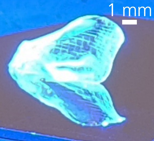
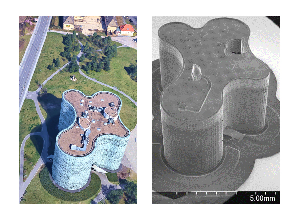
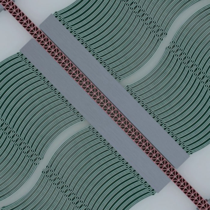
| 24 | Aligned 3D printing on complex or wafer-scale substrates for photonics, acoustics and microfluidics | click here |
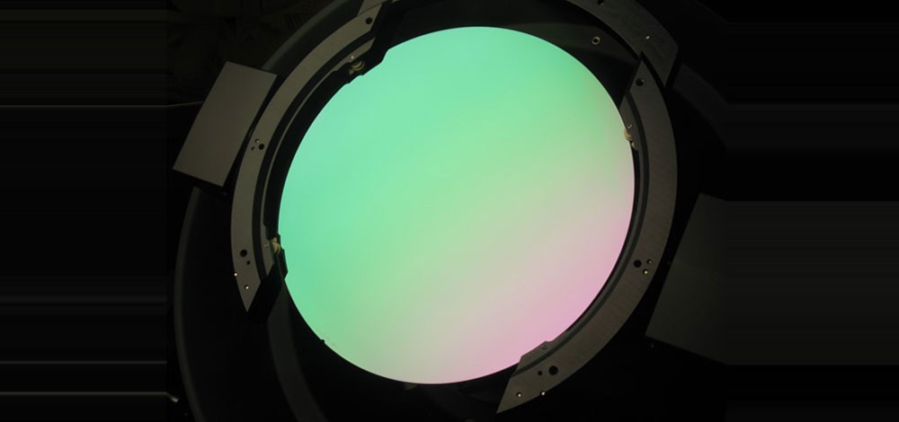
| 23 | Customized BSOI using CMOS compatible Wafergrinder | click here |
| 22 | Two-photon polymerization 3D printing for high-resolution rapid microfabrication | click here |
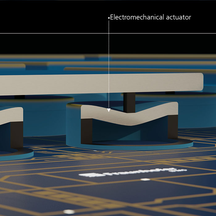
| 21 | MEMS based Micropositioning Platforms - An Introduction to Nanoscopic Electrostatic Drives | click here |
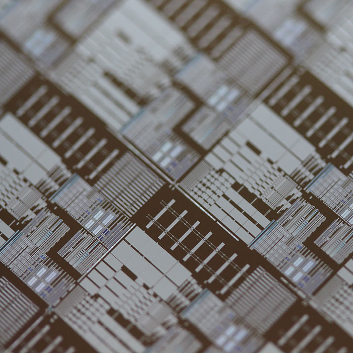
| 20 | 300 mm Semiconductor Analytics: XPS/HAXPES Scanning Microprobe | click here |
| 19 | Managing a High-Mix and Low-Volume MEMS R&D Fab by Applying KPIs | click here |
| 18 | Manufacturing Process Challenges for MEMS Based Holography SLM Devices | click here |
| 17 | Multimodal, Modular and Mobile Sensor System for Improved Patient Monitoring | click here |
| 16 | Development and Fabrication of Leading Edge Thermopile Arrays | click here |
| 15 | Material development for MRAM and FRAM stacks | click here |
| 14 | Neuromorphic Computing for Edge AI | click here |
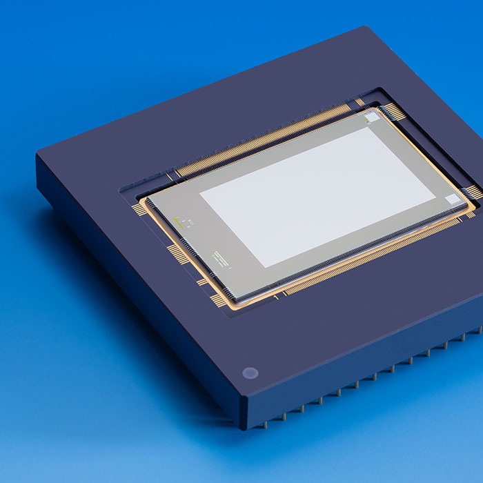
| 13 | Spatial Light Modulators - Status and Potential for Holography | click here |
| 12 | Advanced Technology and Hardware for Next Generation Computing | click here |
| 11 | Optical and Electrical Microsystems for Advanced Biomedical Imaging and Diagnosis | click here |
| 10 | MEMS Technologies and Applications | click here |
| 09 | Low Frequency MEMS Ultrasound Transducers | click here |
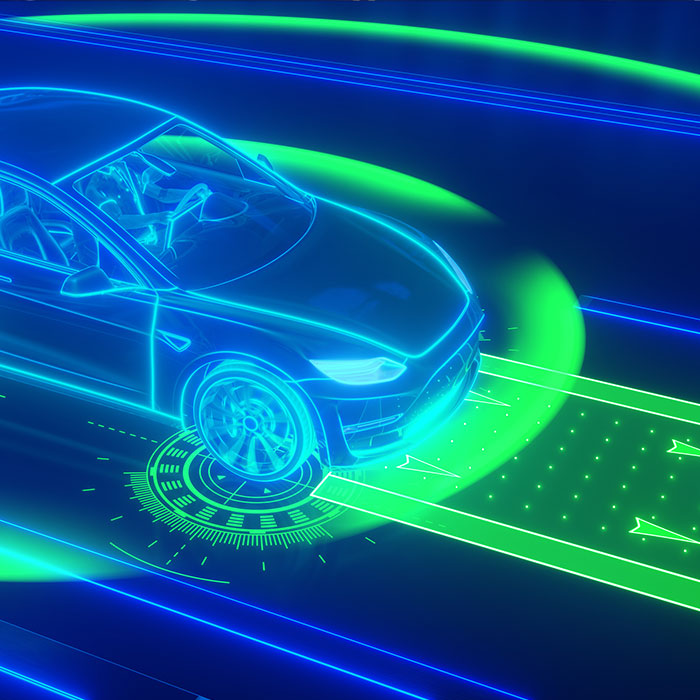
| 08 | MEMS Technologies for Vehicle Environment Detection | click here |
| 07 | Smart Systems for Medical and Health | click here |
| 06 | Capacitive Micromachined Ultrasonic Transducer (CMUT) – From Concept to Device | click here |
| 05 | Fe- FET - A Memory Device for Maximum Integration | click here |
| 04 | Automotive LIDAR Technologies | click here |
| 03 | Fraunhofer IPMS Micro Mirror Arrays - Versatile Spatial Light Modulation | click here |
| 02 | The power of Micropump – A big idea in a small package | click here |
| 01 | Li-Fi - Communication at the Speed of Light | click here |