Branch »Integrated Silicon Systems« (ISS)

Fraunhofer IPMS »Integrated Silicon Systems« (ISS)

The Fraunhofer Institute for Photonic Microsystems IPMS has been successfully conducting research and development in Lusatia since 2012 in a variety of collaborations with regional partners. In accordance with the self-image of the Fraunhofer-Gesellschaft, the institute with its Cottbus-based branch "Integrated Silicon Systems ISS" focuses on the transfer of developments and innovations of application-oriented research to industry as well as a strong networking of the stakeholders. In close cooperation with industry and science, in particular with the Brandenburg University of Technology Cottbus-Senftenberg (BTU C-S), the institute provides decisive impulses for Lusatia with the aim of contributing to sustainable, regional value creation and an efficient economic region.
Fraunhofer in Lusatia

The close relationship between Fraunhofer IPMS and the Brandenburg University of Technology Cottbus-Senftenberg (BTU C-S) has grown over the years. Institute director Harald Schenk holds the professorship "Micro and Nano Systems" at the BTU C-S and conducts research and teaching there in the field of silicon-based MEMS devices and systems based on them. In 2012, the Fraunhofer project group MESYS was founded in close cooperation. Building on its successes, among others, the institute branch of the Fraunhofer IPMS was founded in Cottbus in 2018. In the spin-off Arioso Systems GmbH with operating sites in Dresden and Cottbus, the technology developed by MESYS is used for the product development of miniaturized loudspeakers.

Another activity of the Fraunhofer IPMS in Lusatia is the "Innovation Campus Electronics and Microsensors Cottbus" (iCampµs), a research cooperation together with the four partners BTU Cottbus-Senftenberg, IHP - Leibniz Institute for Innovative Microelectronics, Ferdinand-Braun-Institut- Leibniz-Institut für Höchstfrequenztechnik (FBH) and Fraunhofer Institute for Reliability and Microintegration (IZM). The aim of iCampµs is to jointly develop existing, exploitable results further in the direction of potential products, in particular sensory systems for applications in the fields of Industry 4.0, Agriculture 4.0 and Smart Health. By accelerating the transfer of R&D results, the campus aims to contribute to increasing the innovation and competitiveness of regional companies, research institutions and the Lausitz region as a whole, and to creating jobs in the high-tech sector.

Other joint activities include Fraunhofer project groups for the pre-development of technologies, processes, components and systems for which there will be a need on the part of industry in the next 6-10 years and the Innovation Hub 13 with a focus on networking the players and creating structures that favor the transfer of knowledge and technologies.

Services

At the Integrated Silicon Systems ISS in Cottbus we offer state-of-the-art research in the field of mechanical and electrical characterization including dynamic testing of micro devices, electrostatic actuators, especially for microfluid applications, and terahertz micromodules.

The institute section has several laboratories at the Brandenburg University of Technology Cottbus-Senftenberg (BTU C-S), which are equipped with state-of-the-art measurement equipment for the characterization of devices and subsystems. For this purpose, parts of the laboratory infrastructure will be relocated to a clean room environment. The measurement equipment is used to characterize optical, electrical and microfluidic properties of devices. For this purpose, a digital holographic microscope, an infrared microscope, a terahertz system as well as a wide range of electrical measuring equipment and soon a scanning electron microscope will be available. With a "two-photon lithography system" with up to 300nm voxel size, adjustments can be made in the form of rapid prototyping on microsensors and microactuators.

We are able to perform the following measurements and services both at wafer level and on the individual component:

Digital Holographic Microscope (DHM)

The Digital Holographic Microscope (DHM) captures the entire topographic information of a microscopic sample within a single image acquisition with a height resolution down to 0.2 nm (approx. two atomic layers). This allows fast vibrations to be captured with nanometer accuracy and imaged in 3D. Typical materials are: Metals, silicon, glasses (e.g. optical lenses), silicon, deposited layers on substrates etc. Individual chips as well as entire wafers are measured.

Infrared microscope with lock-in thermography

The infrared microscope with lock-in thermography can register local hotspots down to 0.001°C, which is used for thermal analysis of the encapsulated MEMS chips. Typical samples are: Semiconductor devices, printed circuit boards (PCB), electronic circuits, MEMS elements, individual chips as well as whole wafers.

3D printing using two-photon lithography / two-photon polymerization (TPP)

© Fraunhofer IPMS-ISS
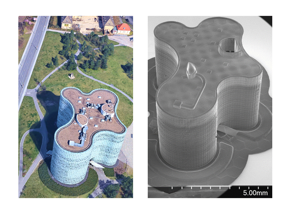
Information, Communication and Media Center (IKMZ) of the BTU Cottbus-Senftenberg printed by means of two-photon lithography at a scale of 1:6400 compared to the original (left).

Our "Photonic Professional GT2" two-photon lithography system from Nanoscribe GmbH allows three-dimensional additive manufacturing of micro- and nanostructures in a photosensitive polymer.  This process is based on the nonlinear optical effect of two-photon absorption, whereby laser pulses from the near-infrared spectral range are focused in such a way that two photons are simultaneously absorbed within a photoresist. The process is thus equivalent to the absorption of a UV photon, which is capable of initiating a polymerization process. This occurs in the transparent photoresist only at the highest radiation intensities and therefore exclusively in a volume (voxel) at the focus of the laser beam. Thus, the movement of the laser focus along a trajectory in all three dimensions enables the generation of almost arbitrary structures and this at resolutions in the submicrometer range.

To enable diverse development tasks, we have an infrastructure at the "Integrated Silicon Systems" (ISS) branch of the institute at the Cottbus site that covers the entire process chain from the design of the component concept, production in the clean room and final examination using optical and scanning electron microscopes. In addition, printed structures can be metallized in our laboratories by means of sputtering.

As a research and development service provider for electronic and photonic microsystems, Fraunhofer IPMS uses two-photon lithography in numerous projects for the production of prototypes. These include the fabrication of:

  • RF and THz MEMS
  • Masters for nano-bead lithography
  • Electromagnetic and acoustic metamaterials
  • Optical surfaces

as well as direct fabrication on our existing MEMS components.


Our services

  • Prototyping
  • Metallization
  • Optical characterization
  • SEM characterization

Technologies

Sensors and actuators

For more information on the technologies at the ISS institute section, please click on the respective tiles.

Components & Systems

Ultrasonic Sensors

Components & Systems

Chemical Sensors

Components & Systems

Optical Sensors

Components & Systems

Electrical Sensors

Components & Systems

Lateral Micromechanical Ultrasonic Transducer (L-CMUT)

Components & Systems

Micromachined Ultrasound Transducers (CMUT)

Contact


Fraunhofer IPMS

Integrated Silicon Systems

Konrad-Zuse-Straße 1
03046 Cottbus

Fraunhofer IPMS

Networks & Collaborations