 Fraunhofer Institute for Photonic Microsystems
Fraunhofer IPMS presents services in the 200/300 mm semiconductor area at Semicon Europa
Semiconductor technology for everyone
Innovative electronics require state-of-the-art technologies and manufacturing processes. For many medium-sized companies, this is an investment that is almost impossible to bear. But thanks to the Fraunhofer Institute for Photonic Microsystems IPMS and its two clean rooms, the latest research results and technologies on 200 and 300 mm wafers are also accessible to smaller companies. The offer ranges from consulting to process development and pilot series production.

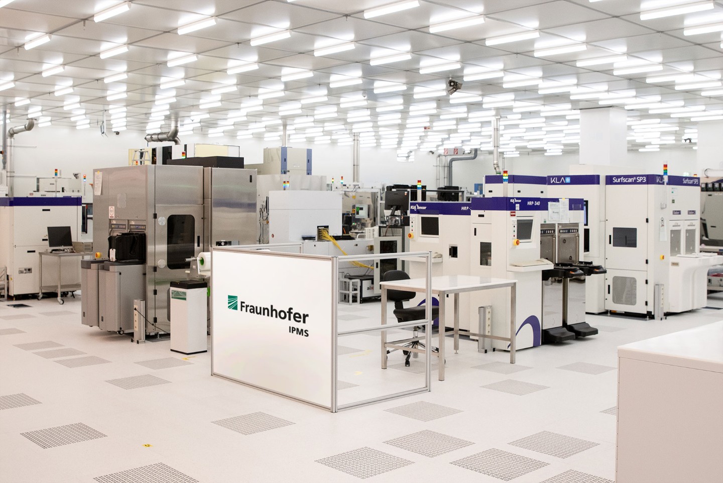
The level of automation and efficiency in industry has increased significantly with Industry 4.0 and the Internet of Things. This requires more and more sensors, actuators, control devices and machine learning systems. The demand for compact, energy-efficient and advanced technologies as well as miniaturized components with innovative functions is increasing. However, the development of many of these technologies involves high costs and the use of a clean room. With its 200 mm research portfolio, Fraunhofer IPMS offers low-threshold access to these cutting-edge technologies and equipment parks, especially for smaller companies.
MEMS technologies and devices on 200 mm wafers
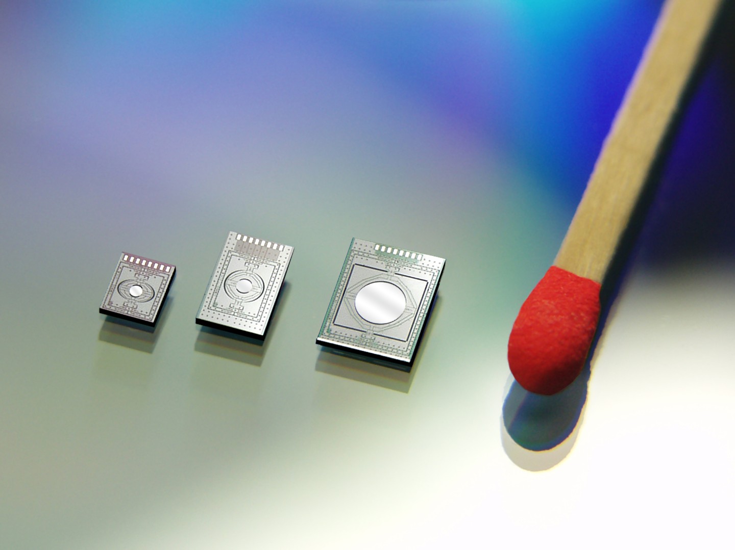
Customers of Fraunhofer IPMS can take advantage of the complete service for the development of micro-electro-mechanical systems (MEMS) and micro-opto-electro-mechanical systems (MOEMS) on 200 mm wafers.
In the field of sensors and actuators, for example, Fraunhofer IPMS develops and manufactures spatial light modulators (SLM) and capacitive ultrasound sensors (CMUT) using sacrificial layer technology within surface micromechanics. In addition, the institute offers high-precision mirrors in volume micromechanics as well as the unique Nano-E-Drive actuation principle, which is used in a wide range of applications. These actuators are based on deep-etched silicon structures with large aspect ratios (up to 1:40 using the Bosch process). They offer high energy efficiency in a small package space.
The technological development and support of MEMS technologies, from single processes to technology modules and complete technology, as well as the process-related support of the equipment in the clean room is provided by more than 100 engineers, operators and technicians. After successful development, the institute offers pilot production or technology transfer support. Fraunhofer IPMS covers the technology readiness levels (TRL) from three to eight.
Start-ups, SMEs and companies without their own Fab in particular can thus benefit from access to high technology at low investment costs.
300 mm semiconductor process and product development for nanoelectronics
Not only 200 mm technologies are developed by Fraunhofer IPMS. With the Center Nanoelectronic Technologies (CNT), the research institute conducts applied research on 300 mm wafers for microchip producers, suppliers, equipment manufacturers and R&D partners.
A variety of Ultra Large Scale Integration (ULSI) level technology developments and services are offered. These include, among others, atomic layer deposition, chemical-mechanical polishing, wafer metallization, wafer cleaning, metrology or nanopatterning. The focus of the R&D activities is on the front end with emphasis on the integration of functionalities in wiring layers (BEoL module). By bundling the competences with Fraunhofer IZM-ASSID (focus on heterointegration and wafer level packaging), which is also active on 300mm, a joint center with a clean room of 4000 m² size was recently established. Focal points are, for example, work in the field of neuromorphic computing, quantum computing and hybrid bonding.
Neuromorphic Computing
Speed, performance, miniaturization and energy efficiency are becoming increasingly important when it comes to enabling Big Data and Artificial Intelligence (AI) applications. Neuromorphic computing offers a promising approach to solving this problem. Neuromorphic chips are modeled on the human brain and have highly interconnected artificial neurons and synapses. The higher computing power of such chips is mainly achieved by the fact that they - just like the neurons and synapses in the human brain - store and process information simultaneously (in-memory computing).
Fraunhofer IPMS is developing innovative technologies and hardware solutions with high energy efficiency using an in-memory computing approach, especially for sensor-related direct data processing on site without transfer to the cloud (edge computing). For different generations of neuromorphic hardware, Fraunhofer IPMS is researching crossbar architectures based on non-volatile memories (e.g. ferroelectric field effect transistors).
Latest research results at Semicon Europa
At the trade fair Semicon Europa in Munich, Fraunhofer IPMS presents its latest research results and technologies from November 15 to 18. Visitors of the fair can talk to the researchers at the Silicon Saxony joint booth #C1-219/11a.
