 Fraunhofer Institute for Photonic Microsystems
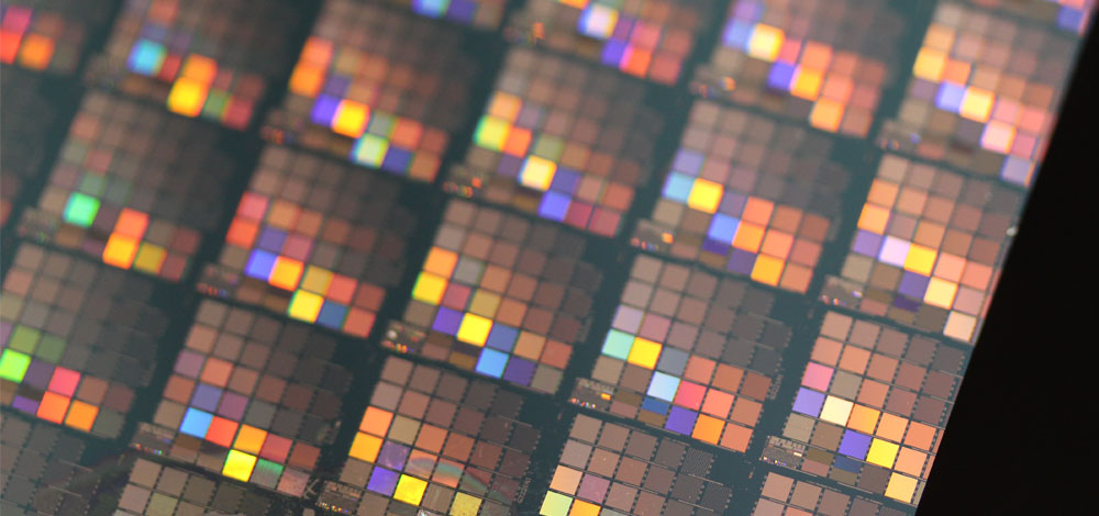
During the volume production of microprocessors, the wiring level plays a key role in ensuring the performance, energy efficiency and reliability of the system. The metallization of the individual layers is realised in various modules in which lithography, etching, cleaning, thin-film, electroplating, furnace and polishing processes play a major role.
At the Fraunhofer IPMS, this complete process line can be mapped and examined individually. The focus here is on copper metallization. In the damascene process, the etched structures are lined with the barrier and copper seed layer, in order to fill them electrochemically with copper in the following plating step through a bottom-up fill, the so-called superfill. After a furnace process, in which larger copper crystal grains are formed, the CMP step (chemical-mechanical planarisation) follows, in which the excess copper is polished away in order to isolate the individual conductive tracks from each other and to create a uniform height. Adapted cleaning processes both before metallization (post etch clean) and after polishing (post polish clean) help to create levels that are as defect-free as possible.
Each of these steps has its own challenges, which are tackled at Fraunhofer IPMS on 300 mm wafers in the respective modules in an industrial and scientific environment in interaction with our own state-of-the-art equipment and material manufacturers as well as with IC manufacturers and in the knowledge of current developments on processes in 28 nm and 22 nm technology nodes and beyond.