 Fraunhofer Institute for Photonic Microsystems
Wafer Cleaning
As the requirements for increased device performance and reliability in VLSI and ULSI silicon circuit technology have become more demanding, techniques to prevent contamination and processes to produce very clean wafer surfaces are critical. Numerous cleaning operations are necessary in the course of semiconductor manufacturing and must be performed at certain critical process steps. To ensure fast, selective, uniform and cost-effective cleaning, the Center for Nanoelectronic Technologies offers a state-of-the-art cleaning platform.
As a link and test environment for suppliers and chip manufacturers, we offer evaluation, screening and optimisation of new chemicals and processes from laboratory scale to testing on our own wafers (2x nm technology nodes).
Our services
- Post Etch Residues Removal (PERR)
- Photoresist stripping & lithography stack rework
- Benchmarking of consumables
- Long-term tests / yield tests
- Post CMP clean (chemistry and consumables)
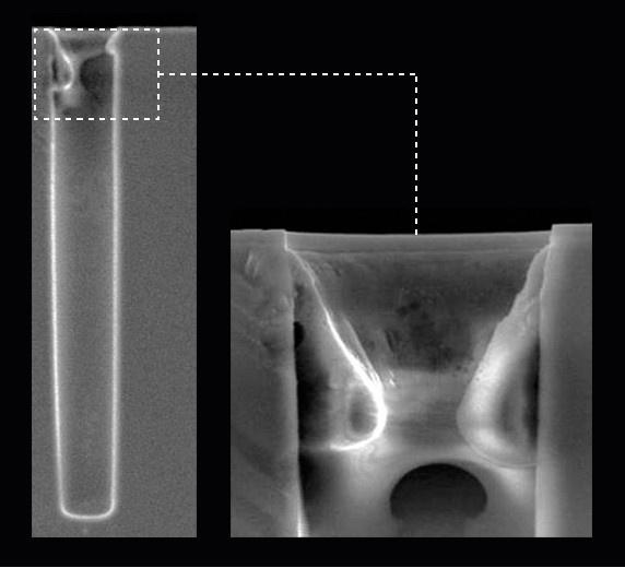
- Removal of polymeric residues after TSV-Etch
- Dual Damascene hardmask-etch