 Fraunhofer Institute for Photonic Microsystems
Project GENESIS minimizes ecological footprint in Europe’s semiconductor industry
A pan-European consortium dedicated to developing sustainable processes and technologies for the semiconductor-manufacturing supply chain announces the launch of the GENESIS project. This integrated, large-scale initiative aims to enable Europe’s chip industry to meet its sustainability goals – from material development to final waste treatment. Fraunhofer IPMS takes a managing role for one of the central work packages in order to minimize chemical waste and reduce emissions.
Fraunhofer IPMS to minimize chemical waste and reduce emissions in the GENESIS project
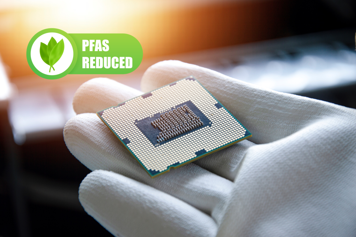
Fraunhofer IPMS takes a managing role for one of the central work packages in order to minimize chemical waste and reduce emissions. In addition, the research institute is investigating the substitution of harmful materials and substances used in semiconductor production. The focus here lies on alternatives for PFAS (perfluorinated and polyfluorinated alkyl substances) and climate-damaging gases in the BOSCH process. The respective project section will examine certain improved recycling techniques, analyze abatement efficiency and even develop new systems.
The mindful use of resources will be central to our efforts in the GENESIS project. We are concentrating on replacing and reducing the emission of climate-damaging gases such as SF6 or NF3. These gases are 10,000 times more harmful than CO2, but are needed in the semiconductor industry. We are also working to reduce the waste produced during chemical mechanical polishing.
