300 mm CMOS Cleanroom

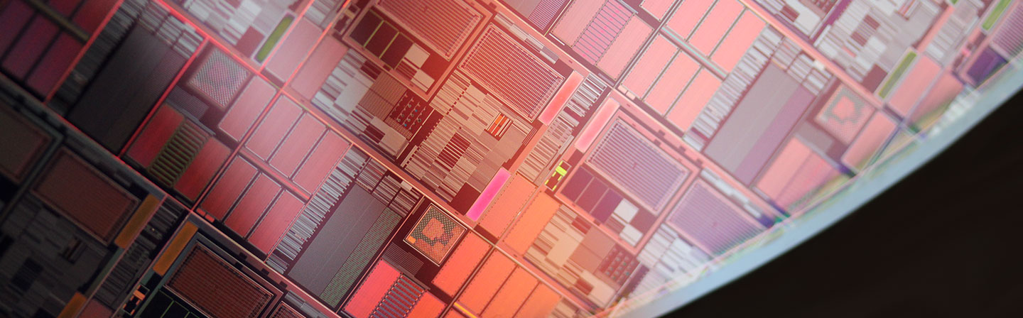
Process and Product Development for Advanced Nanoelectronics

With the Center Nanoelectronic Technologies (CNT), Fraunhofer IPMS conducts applied research on 300 mm wafers for microchip producers, suppliers, equipment manufacturers and R&D partners.

For processing customer orders, 2700 m² of clean room space of class 6 and 3 (according to ISO 14644-1) as well as laboratory space for more than 80 processing and analytical tools are available. The equipment park includes deposition and etching systems as well as inspection and analysis equipment for determining defects and measuring layer properties.

Please select:


300 mm

CMOS Cleanroom Infrastructure


300 mm

Back-End-of-Line Integration (BEoL)


300 mm

Integrated Data Memory

Our Screening Fab Services:


PROCESSES

Leading edge processing and process development for Nanopatterning, ALD, CMP, Wafer Plating and Wafer Cleaning.


EQUIPMENT EVALUATION

Qualification of new equipment, parts and consumables for mass production under industry standard conditions.


WAFER SERVICES

Broker services for blank wafer and structured wafer for further processing including advanced metrology.

Privacy warning

With the click on the play button an external video from www.youtube.com is loaded and started. Your data is possible transferred and stored to third party. Do not start the video if you disagree. Find more about the youtube privacy statement under the following link: https://policies.google.com/privacy

Fraunhofer IPMS - 300 CMOS Cleanroom Tour