Clean Technologies

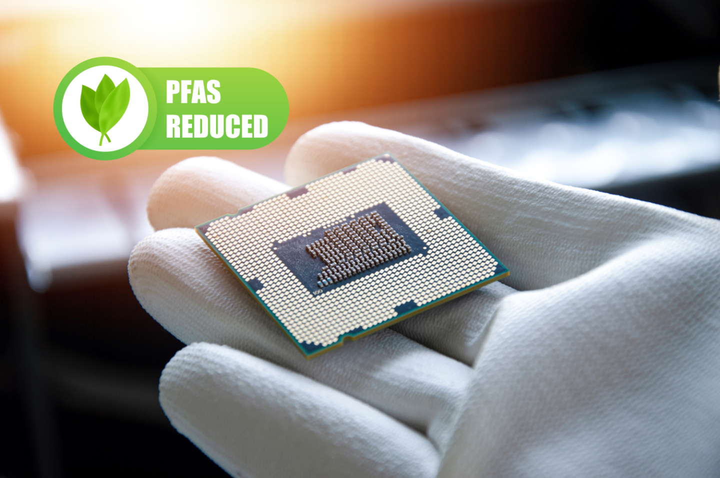
Reducing Greenhouse Gas Emissions in Cleanrooms

Fraunhofer IPMS focuses on reducing the environmental impact of technical gases and refrigerants used in the cleanroom. Through detailed analysis of current consumption patterns, the initiative aims to create transparency and identify optimization potential. At Fraunhofer IPMS, ISO certifications and a modern building management system already enable precise annual tracking of greenhouse gas usage.

Innovative measurement technologies are being developed to record exact gas consumption and continuously monitor exhaust emissions. This includes real-time tracking of unprocessed greenhouse gases, which is essential for calculating their true impact on the climate. The collected data will contribute directly to the organization's overall greenhouse gas (GHG) balance.

Reducing Greenhouse Gas Emissions from Technical Gases in Semiconductor Manufacturing

Initial findings show that fluorinated specialty gases, although used in relatively small quantities, contribute disproportionately to GHG emissions due to their high Global Warming Potential (GWP). One major goal of the project is to determine how much of these gases are actually emitted into the atmosphere versus being consumed or neutralized via scrubbers and burners.

By developing a reliable data collection concept and integrating it into the Fraunhofer GHG balance, the project helps pave the way for greener microelectronics and sustainable cleanroom operations.

Reduction of PFAS in microelectronics production

MEMS components such as Capacitive Micromachined Ultrasound Transducers (CMUTs) are increasingly used in medical diagnostics, industrial automation and non-destructive testing. However, when operating in ambient conditions, these devices are vulnerable to degradation from oxidation and moisture.

Traditionally, hydrophobic coatings like PTFE (Teflon), which belong to the PFAS group, have been used to protect sensitive structures. Due to environmental concerns and regulatory pressure to eliminate PFAS, Fraunhofer IPMS is researching sustainable alternatives like FDTS (fluorodecyltrichlorosilane) that offer comparable protection and performance.

Fraunhofer IPMS research in the field of PFAS reduction:

  • Developing PFAS-free coating processes using less harmful substances
  • Evaluating equipment and procedures to prevent PFAS leakage
  • Identifying alternative materials that maintain high product quality
  • Verifying performance through analytical methods, including hydrophilicity tests
  • Assessing long-term effects and risks of new material classes

Example: Reduction of PFAS (PTFE) in ultrasonic sensors

A key research project investigated replacing a 100 nm-thick PTFE layer in an ultrasound sensor with a few-nanometer FDTS coating applied via atomic layer deposition. The switch increased resonant frequencies of air-coupled CMUTs without degrading performance. These findings enable design optimization to compensate for material changes, helping reduce PFAS use in ultrasonic sensor manufacturing.

Chemical Mechanical Polishing (CMP) without ceria abrasives

Chemical Mechanical Polishing (CMP) is a crucial process in semiconductor manufacturing but also one of the largest sources of CO₂ emissions in chip production. The use of cerium oxide (ceria) in polishing slurries is particularly critical, as it not only has a poor environmental footprint but is also potentially carcinogenic and faces supply limitations. Therefore, solutions to replace this material are urgently needed.

Sustainable CMP solutions developed by Fraunhofer IPMS

Fraunhofer IPMS is actively working on replacing cerium oxide with more environmentally friendly alternatives such as silicon dioxide (silica). Recent research projects have successfully tested a ceria-free slurry on 300 mm wafers, which is an important milestone towards sustainable microelectronics manufacturing.

By optimizing processes and using alternative materials, CMP can be performed without rare earth elements like ceria, without compromising quality or efficiency. This not only reduces the environmental footprint but also enables greater diversification of chip designs in advanced semiconductor technologies.

Development and Evaluation of Eco-Friendly Water-Based Cleaning Technologies for Semiconductor Manufacturing

Semiconductor production has traditionally relied on petroleum-based solvents that pose significant health risks and environmental challenges. Fraunhofer IPMS is developing eco-friendly, water-based cleaning technologies to replace these harmful solvents.

Clean and Efficient Processes for Cleanroom Applications

In collaboration with intelligent fluids GmbH, Fraunhofer IPMS is testing innovative water-based cleaning fluids that effectively remove photoresist residues from 300mm wafers. These formulations are specifically optimized for cleanroom compatibility, process stability, and automation, which are critical factors for industrial semiconductor manufacturing.

Significant Reduction in CO₂ Emissions and Chemical Use

By utilizing water-rich formulations made from renewable raw materials, this new cleaning technology dramatically lowers CO₂ emissions. It also reduces energy consumption and minimizes the use of aggressive chemicals and complex wastewater treatment, supporting a more sustainable semiconductor production.

Substitution of N-Methyl-2-pyrrolidon (NMP)

N-Methyl-2-pyrrolidone (NMP) is a vital solvent in semiconductor cleanroom processes, especially for precise thin-film structuring (lift-off) and photoresist removal. These steps ensure the high quality and performance of semiconductor devices.

Due to its reproductive toxicity and irritant effects on eyes, skin, and respiratory tract, NMP was added to Annex XVII of the EU REACh Regulation in 2018. Since May 2020, the use of NMP in consumer products at concentrations of 0.3% or more has been banned in the EU, driving the semiconductor industry to seek safer alternatives.

Fraunhofer IPMS research for Sustainable Semiconductor Manufacturing

At Fraunhofer IPMS, research focuses on developing safer, effective NMP substitutes that meet stringent semiconductor requirements. Ideal alternatives must enable residue-free removal of both positive and negative photoresists without damaging sensitive layers such as Si, SiO₂, Al, or Ta compounds. They must be compatible with cleanroom wet benches, support ultrasonic cleaning, and have favorable safety profiles including high flash and boiling points.

Three promising candidates have been identified:

  • A water-based mixture containing ethers and alcohols
  • A solvent based on dimethyl adipate
  • A combination of dimethyl sulfoxide and diglyolamine

Ongoing studies at Fraunhofer IPMS evaluate these options to ensure performance parity with NMP while reducing environmental and health risks. Further process adaptation and testing will support a full transition to safer cleaning solutions in semiconductor manufacturing.