 Fraunhofer Institute for Photonic Microsystems
Distributed Manufacturing for Novel and Trustworthy Electronics T4T" Project
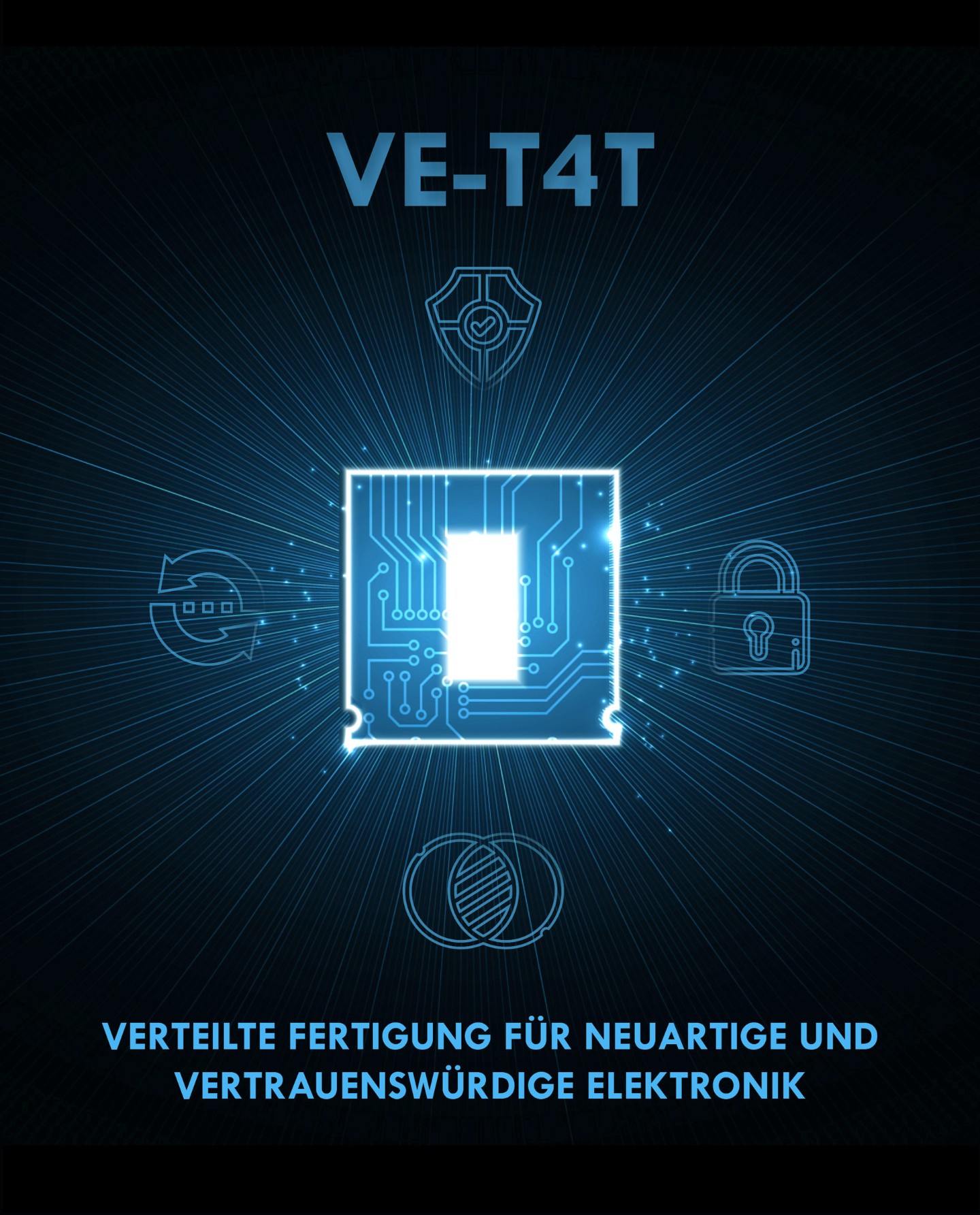
Split manufacturing for trustworthy electronics "Made in Germany"
A consortium of Fraunhofer institutes and well-known German industrial companies is developing a split-manufacturing approach for semiconductor production in the project "Distributed Manufacturing for Novel and Trustworthy Electronics T4T". This will enable the secure assembly of subsystems in Germany and safeguard supply chains.

The secure supply of electronic components is of growing strategic importance for Germany as an industrial location. The increasing relocation of integrated circuit (IC) manufacturing to non-European regions increases the vulnerability to the introduction of malware and espionage functions into components supplied by contract manufacturers (foundries). At the same time, the risk of intellectual property (IP) theft of circuit designs by third parties is increasing. The "Distributed Manufacturing for Novel and Trusted Electronics T4T" project aims to provide domestic industry with tools to access secure supply chains and trusted electronics. Subcomponents adapted to these requirements can still be accessed via existing supply chains (split manufacturing), but the assembly and encoding of the systems will take place in a trusted environment at the German site.
The new technical requirements of this split-manufacturing approach to packaging technology are to be visualized with the aid of various demonstrators. These will illustrate new design flows and methods, adapted manufacturing processes and the individual technical know-how of the project partners involved. In addition to Bosch, Osram, Audi and XFAB, these include NanoWired, Suess, DISCO, IHP, and SIJEDA GbR (associated) as well as the Fraunhofer Institutes IZM-ASSID, IPMS, IIS/EAS and the Technical University of Dresden.
The knowledge gained from the project is intended to make a structural contribution to the standardization of processes in packaging and interconnection technology and, to this end, define new design specifications and tolerance rules for offset and structure sizes.
Within the project, the Fraunhofer Institute for Photonic Microsystems IPMS will address two main topics. On the one hand, the interface between classical front-end (wafer fabrication) and back-end (heterointegration) will be developed and optimized in terms of the split manufacturing approach with regard to contamination management, defect density and process quality. In addition, a modern post-quantum cryptography technique using non-volatile memories (NVMs) will be investigated and tested. This security element, together with distributed manufacturing, should provide additional protection.
The Fraunhofer Institute for Reliability and Microintegration IZM and its branch "All Silicon System Integration Dresden - ASSID" are involved in the production of a 300mm wafer to wafer demonstrator with an encrypted memory element as well as an interposer wafer with integrated chiplets. This is intended to create the technological basis for adapted chip integration. Wafer-to-wafer bonding allows the distribution of system functions to several circuits with close spatial interconnection and thus provides the basis for a packaging technology adapted to subassembly. However, the use of different chip sizes in split manufacturing can lead to obstacles in packaging. Therefore, Fraunhofer IZM-ASSID, with the support of other partners, is developing an approach based on the die-to-wafer bonding process and high-density interconnects that enables the combination of different chip sizes on one interposer. The resulting heterogeneous system is expected to contribute significantly to the establishment of new standards in back-end design. This is because an interposer with bonded chiplets can be used in many different systems.
The Fraunhofer Institute for Integrated Circuits IIS, with its Adaptive Systems Development (EAS) division, will perform the essential work on an end-to-end design methodology. Components and interfaces required for the design flow will be developed, and the necessary chip and package data will be made available in a modular multi-process design kit. Furthermore, Fraunhofer IIS/EAS is significantly involved in the electrical design of the demonstrators as well as in the electrical measurement following manufacturing.
Not only the involved partner companies but also small and medium-sized enterprises will benefit from the achievement of the project goals. The aim is to create potential for them to offer innovative electronics systems and thus increase the technological sovereignty of Germany as a business location. The project has been running since 01.03.2022 and is scheduled to be completed in March 2025. The project volume is €16.44 million and there is funding from the Federal Ministry of Education and Research (BMBF) in the amount of €11.75 million.
