 Fraunhofer Institute for Photonic Microsystems
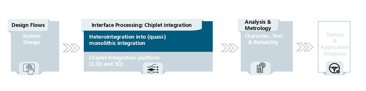
APECS Pilot Line
Heterointegration towards quasi-monolithic integration
APECS Pilot Line: Heterointegration Into Quasi-Monolithic Integration
Heterointegration towards quasi-monolithic integration
Advanced Packaging and Heterogeneous Integration for Electronic Components and Systems
A major component of APECS is the development of quasi-monolithic integration (QMI). In today's world, where technological advances are happening at breakneck speed, it is essential that the integration of different technologies is also at the highest level. This is where quasi-monolithic integration comes into play - a groundbreaking method that breaks down the boundaries between back-end and front-end in microelectronics.
Quasi-monolithic integration refers to a technology in which different functional chiplets (CMOS, MEMS, non-silicon) are integrated into an almost monolithic system. In this technology, these integrated chiplets are arranged and connected with a common interconnect stack on an active or passive wafer substrate and then contacted within the front-end line. This allows the highest contact densities to be achieved. This maximizes the benefits of each technology while minimizing the challenges of integration.
Privacy warning
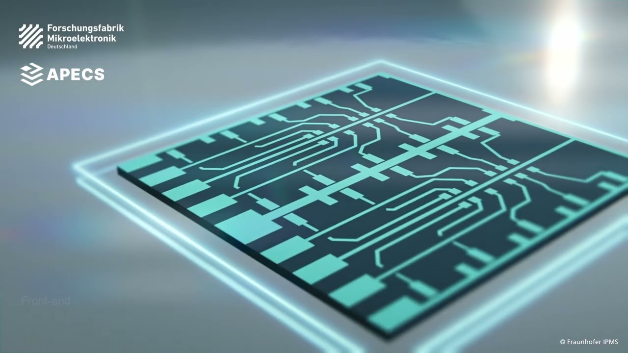
With the click on the play button an external video from www.youtube.com is loaded and started. Your data is possible transferred and stored to third party. Do not start the video if you disagree. Find more about the youtube privacy statement under the following link: https://policies.google.com/privacyHeterointegration into quasi-monolithic integration
Fraunhofer IPMS in APECS: Heterointegration into quasi-monolithic integration
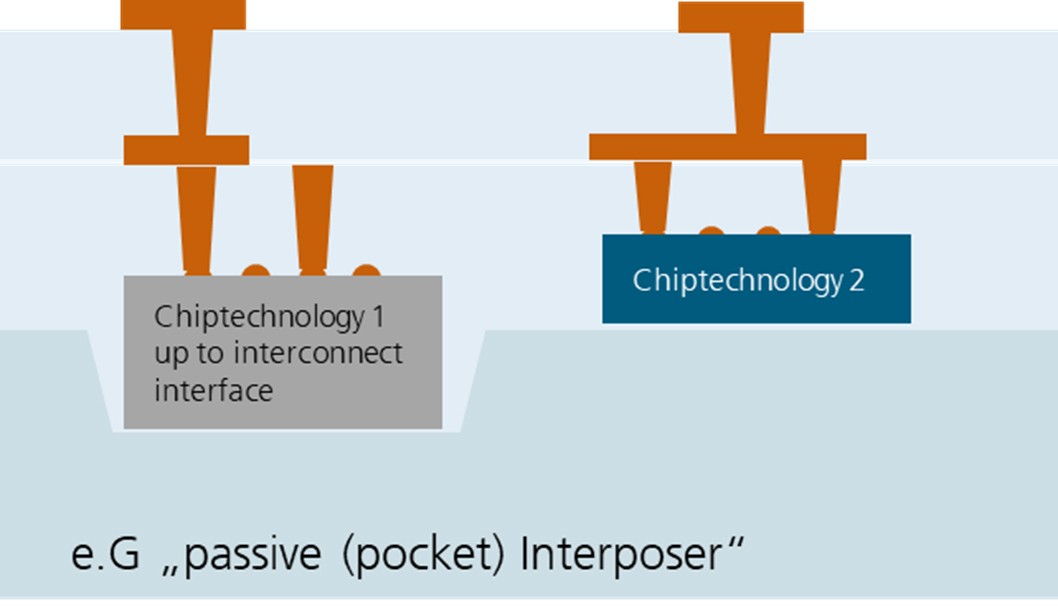
Example of quasi-monolithic integration with common ILD and interconnect technology (multilayer; thermal coupling; seamless PDK/ADK, ...)
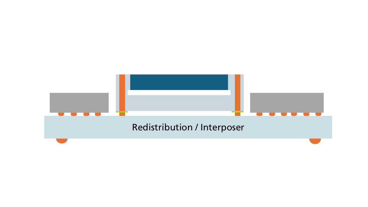
Chiplet integration interface for MEMS devices.
A key part of our contribution to APECS is the development of quasi-monolithic integration (QMI), which will set new standards in chiplet integration technology. The key strength of QMI lies in its ability to combine different materials and technologies in a highly integrated way to create an extremely high performance and reliable end product. In contrast to fully monolithic systems, QMI allows for greater flexibility and customization.
Advantages of QMI
- Performance: The tight integration of different elements significantly increases the performance of the system. Signal losses and delays are minimized, resulting in faster and more efficient data processing.
- Reliability and durability: QMI systems are characterized by increased reliability and longer service life, as mechanical failures are reduced due to the tight connection of the components.
- Compactness: QMI saves considerable space as the elements are integrated almost monolithically.
- Cost efficiency: The QMI combination of chiplets enables cost-efficient maximum integration with fast innovation cycles
These advantages predestine quasi-monolithic integration for innovations such as highly integrated SOC (systems-on-chip) for AI applications (sensor AI) as well as intelligent transceivers with high bandwidth.

3D printing of a demonstrator of quasi-monolithic integration with chiplet in the pocket.
Our contributions in the field of chip manufacturing for III-V optoelectronic components:
- Interface / Dicing
- CMOS-compatible MEMS/µLED
- Interface/ Pockets / TSV (Through-Silicon-Vias)
- Scribing
- Cutting
Our contributions in the field of Opto Carriers:
- Wiring
- Positioning / Bonding
- Planarization
- Metallization
- µTSV (Micro-Through-Silicon-Vias)
- Interface