Back End and Packaging

Back end and packaging competencies at Fraunhofer IPMS.

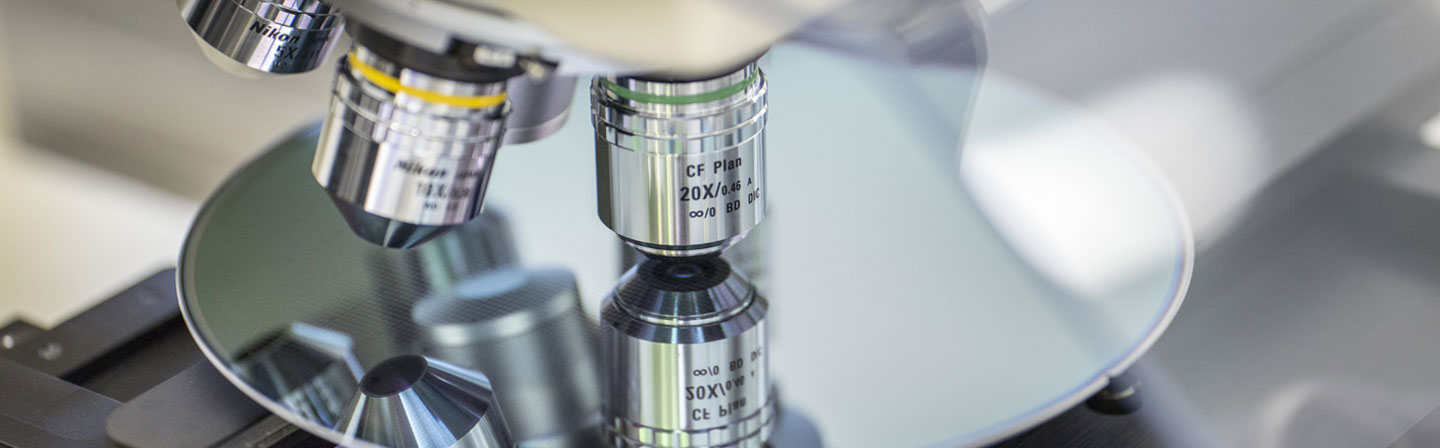
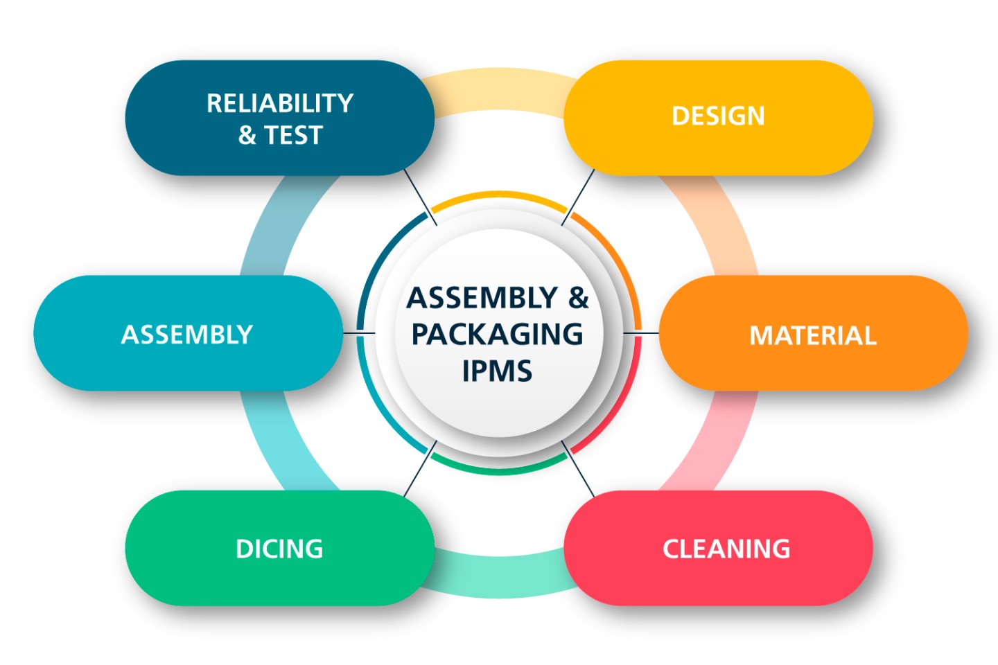
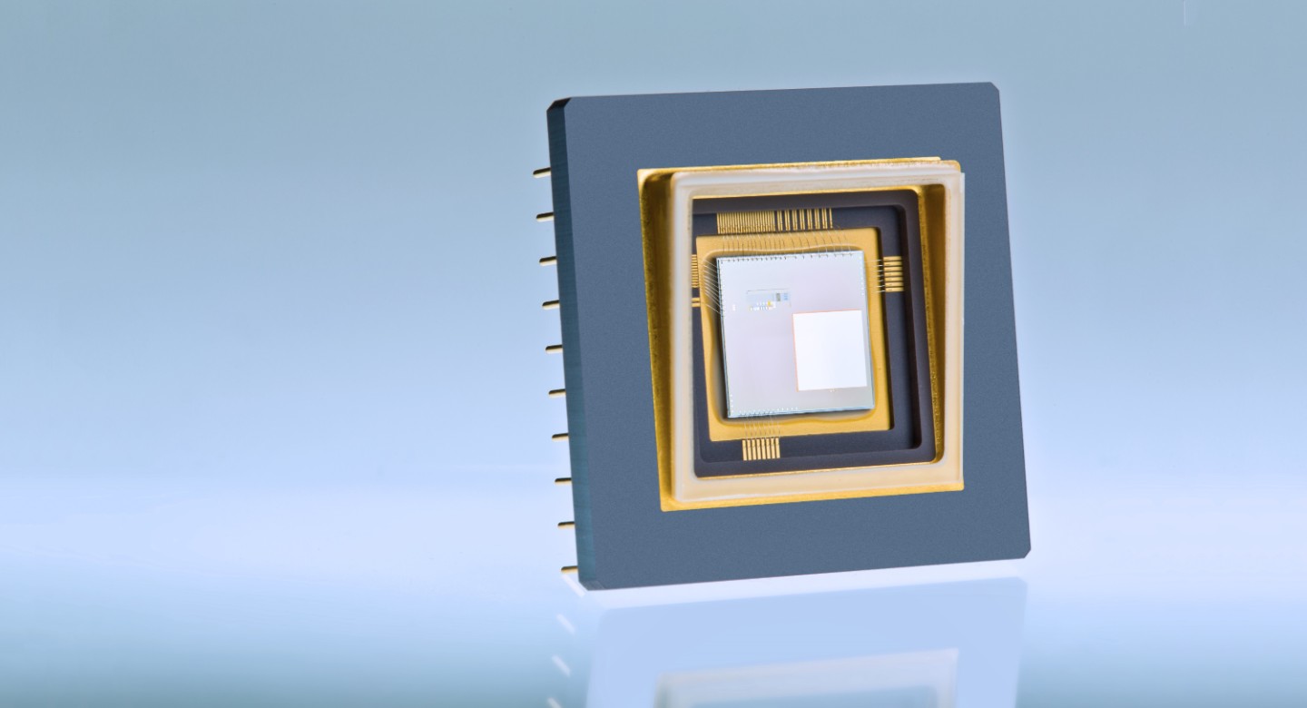
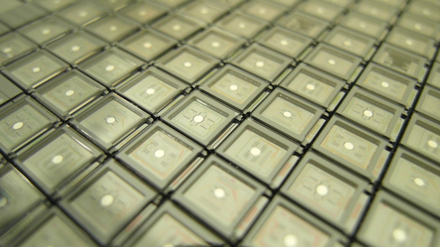
Highly sensitive electronic components are the drivers of modern technology. This requires increasingly complex processes in backend and packaging technology as well. 
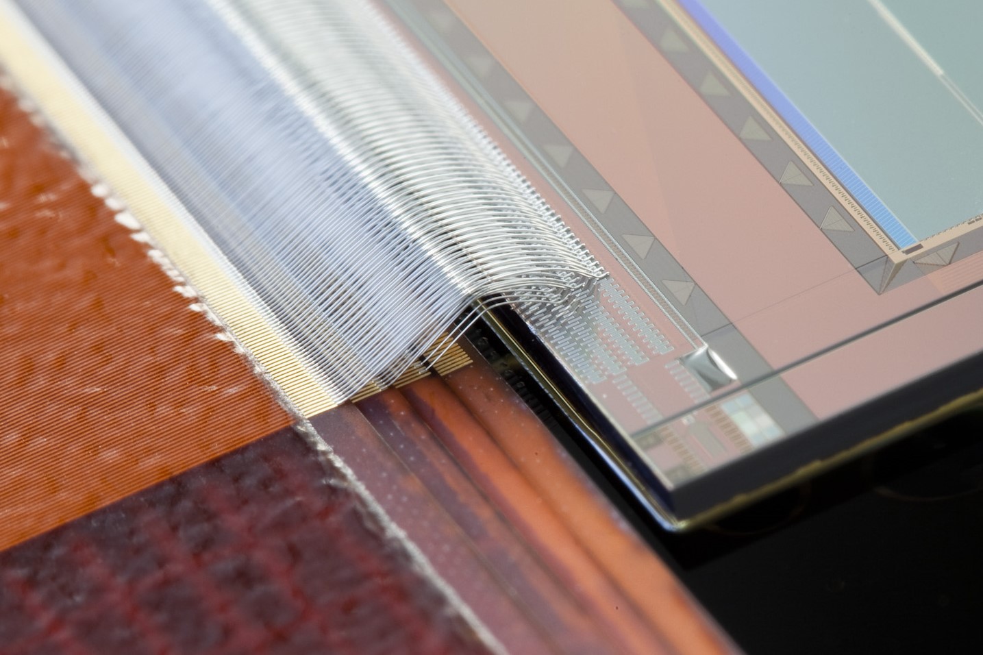
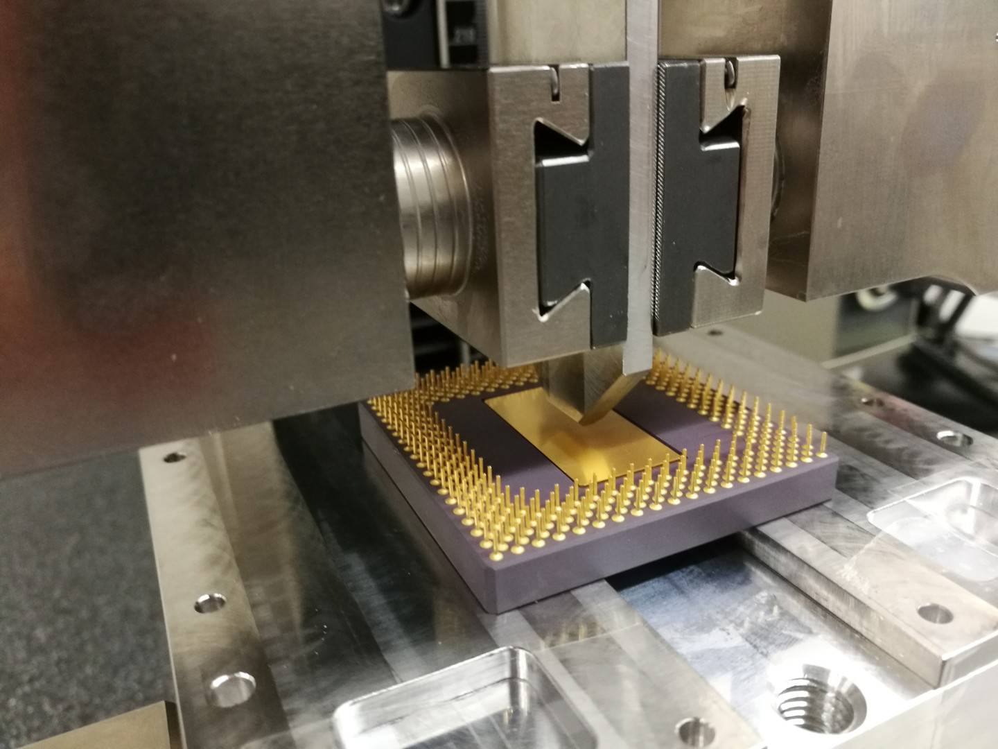
Fraunhofer IPMS offers development services to help our customers create innovative products. We provide support from the design to the final module in quantities starting from one. The system design using MEMS, electronics, optics and other photonic components and the processes for assembling the systems in the smallest volumes go hand in hand. Fraunhofer IPMS has the necessary expertise in chip-package co-design and the required equipment for the backend and micro-assembly and offers as a service both individual process stages and complete development up to small series. Possible applications are MEMS and MOEMS of any kind, optical devices like laser or photodiodes, sensor or bio applications and many more. 

Design

© Fraunhofer IPMS
CAD model of a MEMS package

Upon request, we develop and support package- and system solutions from the very beginning. This can include the housings, substrates, alignment tools, encapsulation, and even customer-specific mountings for microassembly, among other things. Extensive software expertise enables realistic design in 3D CAD, as well as numerous simulations, from optical beams to stress analysis and other FEM simulations. If required, material evaluations are carried out in advance, e.g. of adhesives, sealants or contacting systems. Precise data preparation with traceability of all process steps and materials through our database is also part of our services, as is the provision of all production-relevant data for suppliers.

Dicing

© Fraunhofer IPMS
Diced glass-/silicon wafer stack

The dicing of chips is a major challenge for highly sensitive components like MEMS. Fragile structures and assemblies must not be damaged during the mechanical separation process. Here, IPMS offers numerous protective systems, such as foils and varnishes, which protect the components during cutting. For the separation process, we can offer our customers a high-precision double-spindle saw, which enables the cutting of a wide range of materials (silicon, glass, ceramics, composites and even metal) as well as the creation and opening of cavities and other special shapes on the wafer. In addition, we have the capability of wafer edge trimming at the site.

Chip assembly and contacting

© Fraunhofer IPMS
Die bond
© Fraunhofer IPMS
Multilayer wire bond

Following dicing, IPMS offers its customers the possibility to directly follow a pick and place process in order to re-sort the diced wafers according to customer specifications (e.g. into Waffle Packs or GelPak®).

In addition, we offer high-precision component assembly according to customer specifications. Adhesives, sealants and caps can be dispensed at three independent machines at the site. A precise and reproducible stamping process is also available. The assembly of components on customer-specific interposers and substrates is carried out with high precision down to < 1 µm at 3 sigma. In addition to conductive bonding during assembly, IPMS and its partners have a multi-level wire bonding process available. This allows for a reliable connection even of components with an extreme high number of contacts.

Reliability and test

© Fraunhofer IPMS
Reliability test of a PGA-package

Besides optical and electrical inspection, numerous methods are available at the IPMS for evaluating the packaging results. In addition to the examination of bonding technologies by means of tensile, shear and compression tests, vibration as well as climatic tests (temperature, humidity, UV irradiation) can also be carried out to analyze the reliability of assemblies.