 Fraunhofer Institute for Photonic Microsystems
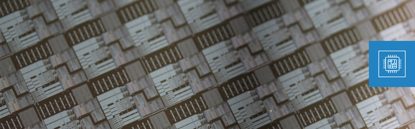
Advanced 300 mm Semiconductor Services for Memory, AI, and Quantum Technologies

From edge AI hardware and Industry 4.0 to quantum computing, next-generation computing technologies require advanced microelectronic solutions that combine high performance, energy efficiency, and scalable manufacturing.
At the Center Nanoelectronic Technologies (CNT) of Fraunhofer IPMS, we provide 300 mm wafer services and develop industry-ready microelectronic solutions on state-of-the-art 300 mm CMOS wafers. Our expertise supports semiconductor manufacturers, suppliers, equipment providers, and R&D partners in accelerating innovation and enabling reliable technology transfer from development to production.
300 mm Wafer Services for Advanced Semiconductor Development
Our 300 mm wafer services cover the development, prototyping, and validation of advanced semiconductor technologies for next-generation applications.
- 300 mm CMOS process modules and custom test chip development
- Nanopatterning and e-beam lithography
- Metallization and process integration
- Advanced metrology and materials characterization
- Semiconductor manufacturing process optimization
MRAM Foundry and Emerging Memory Technologies
As a leading innovation partner in advanced memory systems, CNT supports the development of MRAM foundry technologies and next-generation non-volatile memory solutions, including:
- MRAM (Magnetoresistive RAM)
- RRAM (Resistive RAM)
- FeRAM (Ferroelectric RAM)
Our work focuses on high-density, low-power memory architectures for industrial electronics, automotive systems, embedded devices, and AI applications.
Edge AI Hardware and Energy-Efficient Computing
For intelligent industrial systems, we develop edge AI hardware and energy-efficient AI accelerators that enable fast, low-latency data processing directly at the device level.
- Neuromorphic computing architectures
- Low-power AI chips for industrial automation
- Embedded hardware for real-time sensor data processing
- Scalable semiconductor solutions for Industry 4.0 environments
Semiconductor Innovation for Quantum Computing
CNT is also active in future-oriented research areas such as quantum computing hardware, with expertise in:
- CMOS-compatible quantum components
- Cryogenic control electronics
- Material optimization for quantum devices
By combining applied research with industrial-scale 300 mm wafer processing, Fraunhofer IPMS enables partners to develop breakthrough semiconductor technologies for tomorrow’s computing platforms.

