Fraunhofer IPMS at MEMS & Imaging Sensors Summit 2022
Miniaturized components of Fraunhofer IPMS
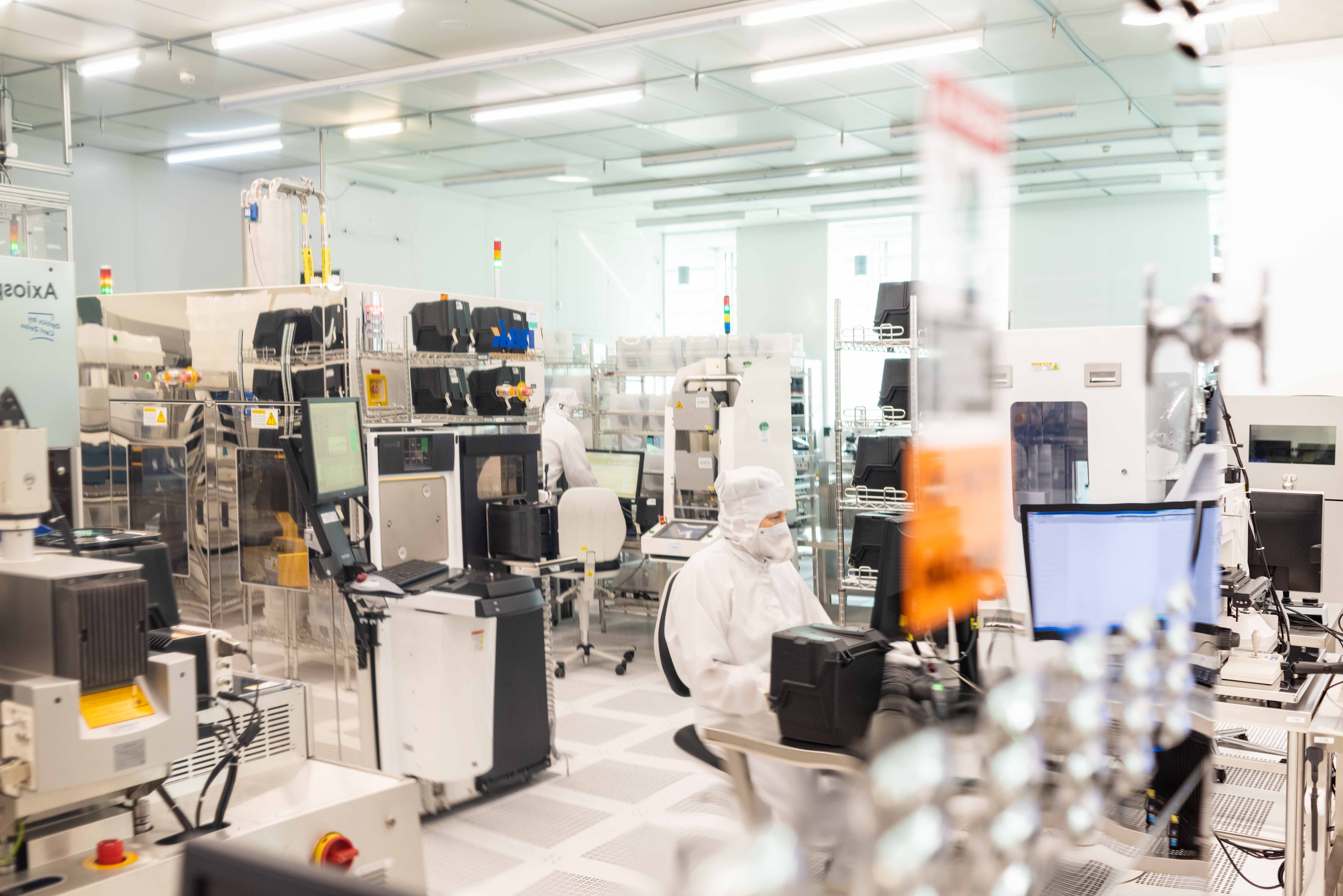
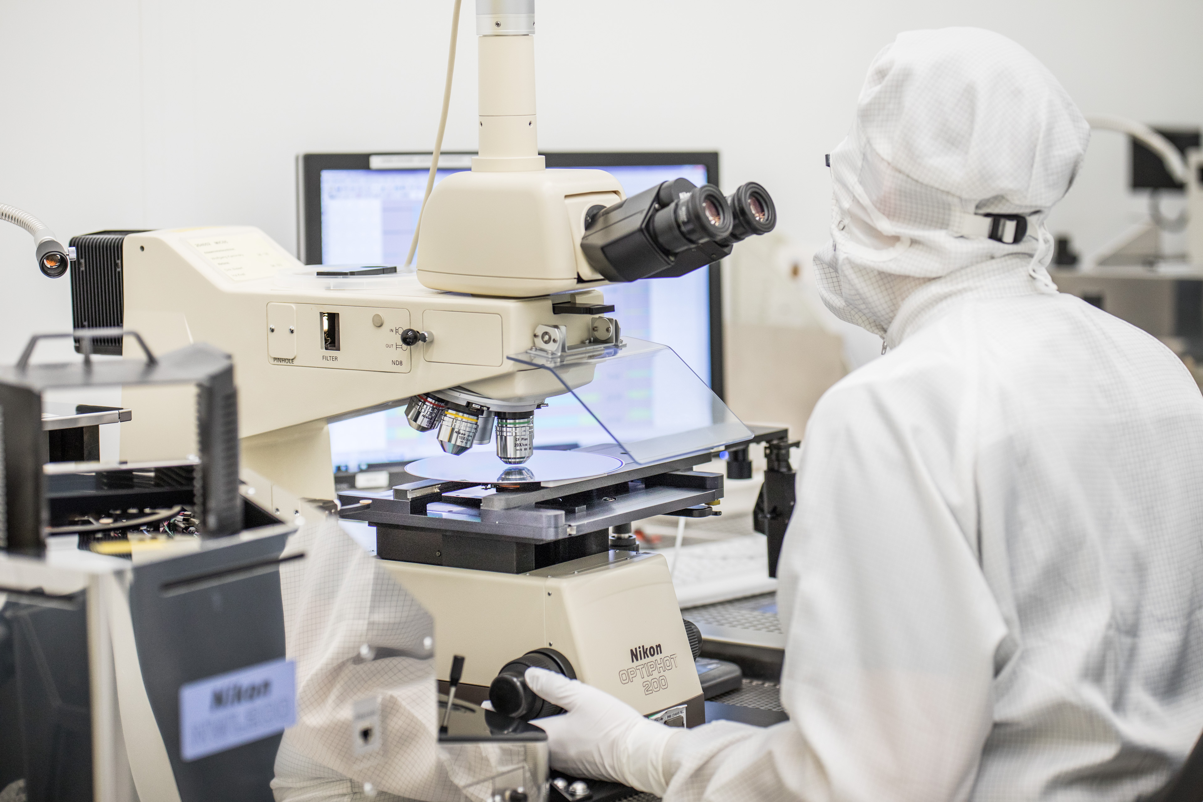
Highly sensitive electronic components are the drivers of our digitalized world. Micro-electro-mechanical systems (MEMS) open up new possibilities for miniaturization in wide-ranging application areas. With its state-of-the-art 200 mm clean room, Fraunhofer IPMS offers the complete value chain for MEMS as well as optical components MOEMS (Micro-Opto-Electro-Mechanical Systems). The range of services extends from consulting on feasibility through initial demonstration at wafer level to pilot fabrication with manufacturing capacities of more than 1100 waferstarts per month.
Under the motto "Intelligent Sensing for Better and Smarter Living", the Fraunhofer IPMS is presenting its comprehensive expertise in the field of 200 mm microelectronics at this year's MEMS Summit in Grenoble. In addition to the conceptual design, development and fabrication of MEMS and MOEMS devices, Fraunhofer IPMS possesses the know-how for the fabrication of individualized BSOI wafers, the electrical characterization of devices and develops suitable packaging solutions following the fabrication. For customers, in particular start-ups, medium-sized companies and companies in niche markets without their own fab, this provides access to high technology.
Sustainability in microelectronics manufacturing
Climate change does not stop in the semiconductor industry. Therefore, Fraunhofer IPMS focuses on sustainable value chains and devices and evaluates, for example, climate-friendly alternatives for critical materials and processes. In the BMBF-funded project "Competence Center GreenICT@FMD", resource minimization in electronics production is being advanced together with partners from the Research Fab Microelectronics Germany (FMD). In addition to energy-saving sensor edge cloud systems and communication infrastructures, Fraunhofer IPMS focuses in particular on resource-optimized microelectronics production.
Through its expertise, Fraunhofer IPMS offers a broad spectrum with comprehensive services for manufacturers of equipment, IC and material to implement resource-optimized and environmentally friendly electronics production. In the field of processing, the institute supports its customers with consulting and development services targeting resource-optimization, especially in the area of lithography and wet processes. This includes both the investigation of alternative materials (e.g. the investigation of cerium oxide free slurries for CMP processes) and their consumption reduction as well as the optimization of energy consumption to reduce the CO2 impact.
Presentation at the MEMS & Imaging Sensors Summit 2022
Jörg Amelung, deputy director of the Fraunhofer IPMS, will talk about future-oriented devices in the lecture "Fast Characterization of Hydrogen-Natural Gas Mixtures with Micromachined Ultrasonic Sensors". The talk will begin at 2:40 p.m. on Sept. 7. Afterwards, there will be the opportunity to talk to Fraunhofer IPMS experts at booth #37.
 Fraunhofer Institute for Photonic Microsystems

