 Fraunhofer Institute for Photonic Microsystems
Insight into Nano Depth - New Fraunhofer IPMS X-ray photoelectron spectrometer enables tiny particle analysis
With billions of minuscule components transmitting important information and signals to progressively smart devices housed on their surfaces, silicon chips are the nerves cells of artificial intelligence. Semiconductor chips are built into every smartphone and are becoming smaller, increasingly powerful and more efficient.
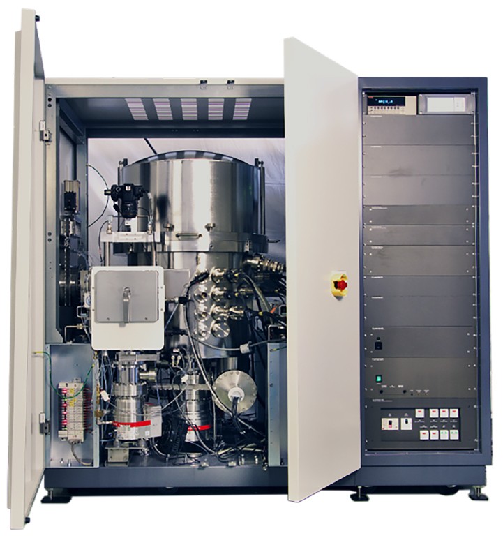
Because surface structures reaching into nanometer range are no longer visible to the naked eye, Fraunhofer IPMS has acquired a new X-ray photoelectron spectrometer (XPS) from Physical Electronics GmbH. This tool will be used to analyze the surface of silicon chips and perform experiments in the nano range.
Fraunhofer IPMS Chief Developer Benjamin Uhlig explains, “With the new Quantes spectrometer from Physical Electronics GmbH, we can examine surface features, thin-film structures and contaminations down to the nano range without causing any damage. Examination in this area is important in order to analyze the exact chemical composition of the chip surfaces. This ability enables us to better understand processes for the manufacture of semiconductor chips as well as optimize chip properties in the future.”
Versatility is another advantage of the new spectrometer. In addition to carrying out conventional XPS measurements with an AI X-ray source, we can now perform analytical experiments with extended depth. An additional Cr x-ray source makes this possible, offering analysis depths (approx. 22 nm) that are around three times as high as those achievable with a AI X-ray source (approx. 7 nm).
Uhlig continues, “Thanks to the short-wave spectrum, we can analyze transitional metals very well. The system can be used to clean the sample surface as well as for depth profiling. In addition, temperature tests from -120°C to 300°C as well as trials with electrical contacting samples can be carried out.”
Samples can also be placed in the chip atmosphere. Electron imaging of the system allows for very precise positioning on structured samples. The new Fraunhofer IPMS XPS system can be used to conduct a wide variety of comprehensive analyses. At the same time, Fraunhofer IPMS offers companies cooperation opportunities within the scope of industry-oriented research.
Fraunhofer IPMS has invested in the X-ray photoelectron spectrometer as part of the Microelectronics Germany research project. Funded by the Federal Ministry of Education and Research, this investment aims to promote Germany as a science and technology location.
Background Information
Based in Dresden, Fraunhofer Institute for Photonic Microsystems (IPMS) provides future-oriented solutions for industrial manufacturing and automation as well as medical technology for an improved quality of life. Over 350 IPMS scientists and engineers perform at the highest level of excellence in the fields of optical sensors and actuators, integrated circuits, wireless data communication and microelectronics.
We develop innovative MEMS components and microelectronic assembly parts on 200 and 300 mm wafers in our two ultra-modern cleanrooms and complete them with the support of our cooperation partners at our four locations in Dresden, Cottbus and Erfurt. In doing so, we build and depend on long-term relationships with our project partners.
The largest cross-location R&D association for microelectronics in Europe, the Research Fab Microelectronics Germany (FMD) is a unique driver of innovation providing a unique variety of skills and infrastructure. The FMD bridges the gap from basic research to customer-specific product development. Made up of the Fraunhofer Group for Microelectronics in cooperation with the Leibniz FBH and IHP institutes, the joint project is funded by the Federal Ministry of Education and Research.
Information: https://www.forschungsfabrik-mikroelektronik.de
Physical Electronics GmbH (PHI) predominantly provides measurement systems for surface analysis and characterization