Fraunhofer Institute for Photonic Microsystems
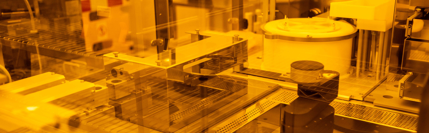
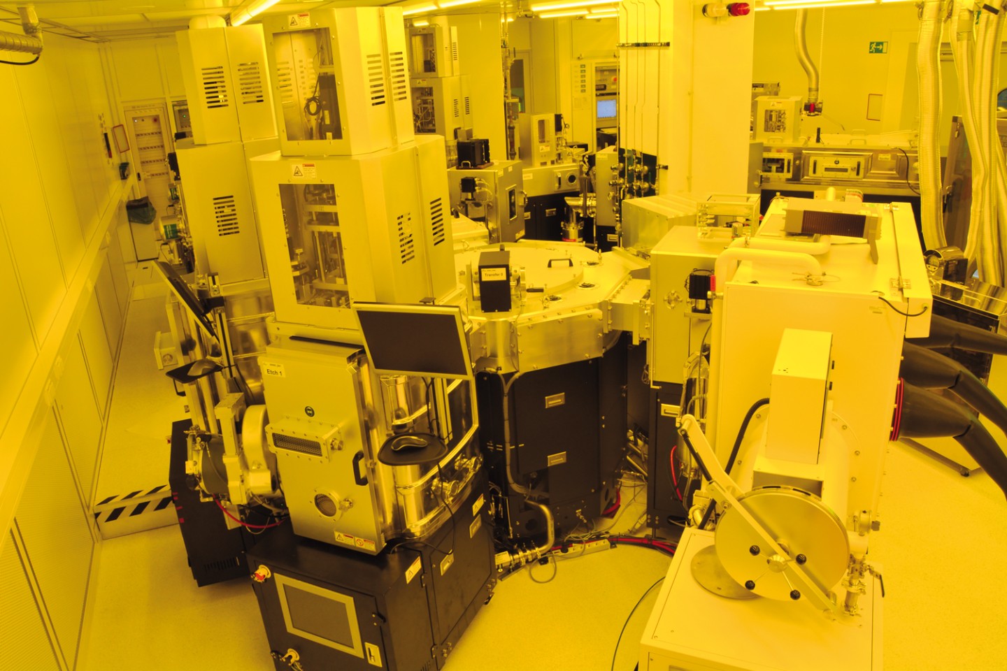
View of a vacuum coating system in the microdisplay cleanroom.
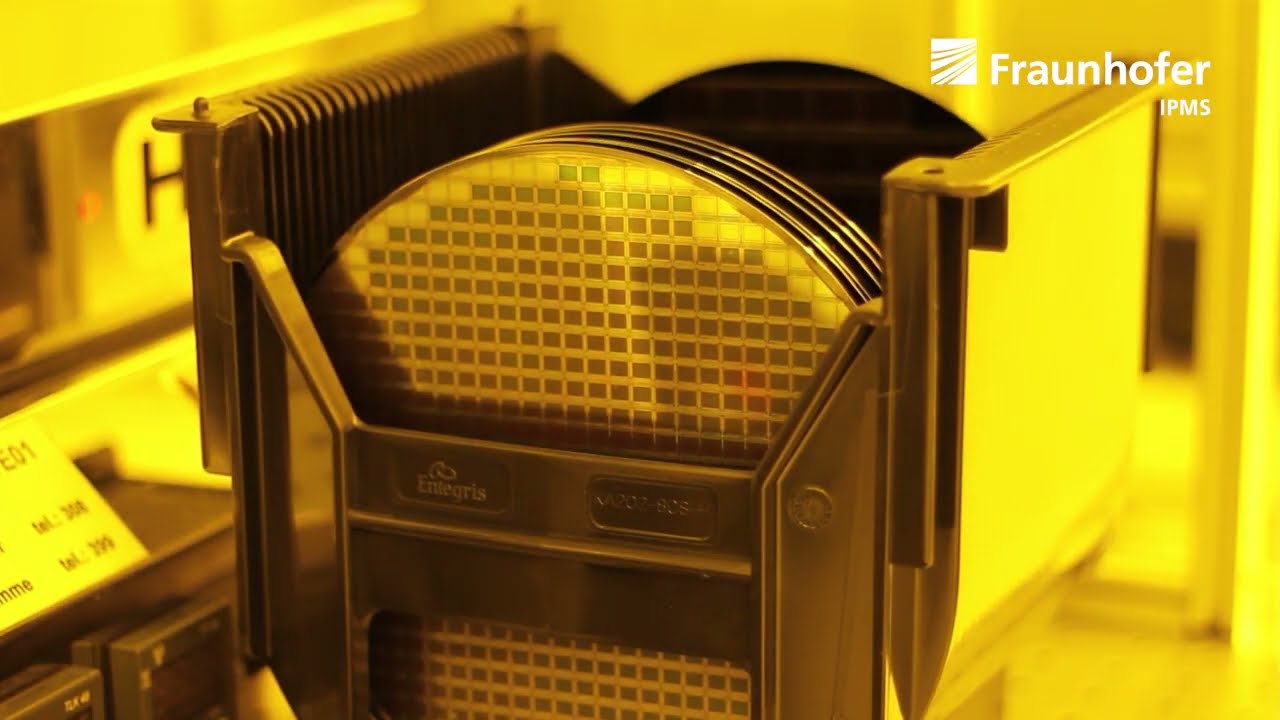
In our microdisplay cleanroom, we offer customers a variety of processes for research, development and pilot production of OLED microdisplays and sensors. Our work focuses on the production of thin films in the nanometer to micrometer range for light emitters and photodetectors as well as their structuring. In addition, various analytical methods for layer characterization are available.
Our microdisplay cleanroom capabilities
- 300 m² class 5 clean room (according to ISO 14644-1)
- 200 mm pilot line for organics-on-silicon (e.g. OLED, OPD, sensor materials...)
- R&D, prototyping, small series up to typically 10'000 wafers per year
- Substrates: silicon, CMOS, glass, III-V or wafer composites
- Thin film deposition by thermal evaporation, ALD, electron beam, sputtering, spin coating
- Structuring by shadow masks (min. structure sizes up to 50µm, positioning accuracy ± 3µm), photolithography (1:1), lift-off, argon milling
- ALD thin-film encapsulation
- Wafer-to-wafer bonding processes, positioning accuracy ± 1µm
- Optical characterization: Ellipsometer, Surfscan, AOI,...
- Electro-optical test at wafer level: wafer prober, double side prober
- Various laboratories for optical characterization at device level