 Fraunhofer Institute for Photonic Microsystems
In the joint research project NEST (New Screening Tool for Efficient Semiconductor Manufacturing), Fraunhofer IPMS, Fraunhofer IZM, and DIVE Imaging Systems GmbH are working within the GreenICT@FMD competence center to make semiconductor production more efficient, cost-effective, and sustainable. The focus is on introducing hyperspectral imaging as an advanced screening tool for wafer inspection and process optimization.
Semiconductor production involves up to 1,500 complex process steps, including etching, deposition, and lithography, which require extremely rigorous quality control. Up to 50% of these steps are dedicated to metrology, and thousands of control wafers are used monthly. This leads to high resource consumption, increased CO₂ emissions, and added cost.
The NEST project revealed that targeted inspection technologies can significantly reduce the environmental footprint of chip manufacturing. In a 28 nm node with 25,000 wafer starts per month, the deployment of hyperspectral imaging could reduce control wafer usage by at least 25%, cutting CO₂ emissions by over 118,000 kg/month. Additional benefits include reduced water and chemical usage, minimized tool load, and increased wafer yield due to early defect detection.
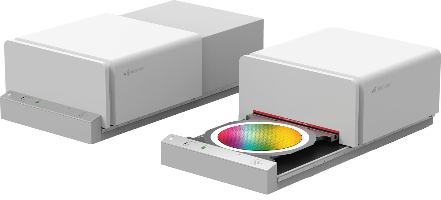
Cleanroom-Ready Hyperspectral Inspection by DIVE and Fraunhofer IPMS
The DIVE VEpioneer® inspection system is the first of its kind to operate reliably in industrial cleanroom environments. It combines optical spectroscopy and AI-based image analysis to detect surface deviations and contamination within just 20 seconds, non-destructively and without halting production.
Fraunhofer IPMS provides critical expertise in cleanroom qualification and optical design, enabling the system’s integration into semiconductor fabs. Following the project's conclusion, the VEpioneer® remains in operation at the Fraunhofer IPMS Center Nanoelectronic Technologies (CNT) for continued evaluation and joint development efforts, including automation of wafer handling and real-time data integration.