Data is the foundation of modern digital industries. From AI and edge computing to industrial automation, the demand for fast, scalable, and energy-efficient non-volatile memory continues to grow. Today, most data is stored as magnetic bits in hard disk drives—an established technology developed more than 50 years ago. However, conventional storage solutions are reaching fundamental scaling and performance limits, restricting further increases in storage density, speed, and power efficiency.
Next-Generation Memory Based on Spintronics
Magnetic Random Access Memory (MRAM) is one of the most promising next-generation memory technologies. Built on advances in spintronics, MRAM stores information using the electron’s spin instead of charge alone. This enables:
- True non-volatile memory
- High switching speed
- Low power consumption
- Excellent endurance
- CMOS compatibility
In addition to MRAM, concepts such as Racetrack Memory (RTM) demonstrate how spin-based devices can enable ultra-high-density storage architectures.
Spin-Orbit Torque and Charge-to-Spin Conversion
A key technological challenge in spin-based memory systems is the efficient charge-to-spin and spin-to-charge conversion. These processes are driven by spin-orbit coupling effects and are essential for spin-orbit torque (SOT) MRAM and racetrack memory devices.
Materials with high spin Hall angles are critical to reduce switching currents and enable low-power MRAM devices. Research into advanced materials and optimized layer stacks is therefore central to improving device performance and scalability.
From Materials Research to Scalable Manufacturing
Our research focuses on bridging fundamental spintronics with industrial semiconductor manufacturing. We investigate:
- Scalable MRAM device architectures
- Nanoscale fabrication processes
- Spin-orbit torque efficiency
- Materials with enhanced spin Hall effects
- Integration into CMOS-compatible process flows
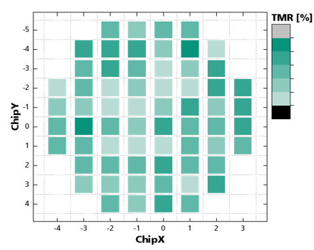
We fabricate and characterize single MRAM cells and nanoscale device arrays using established semiconductor materials and processes. By studying scaling behavior at technologically relevant dimensions, we identify fundamental obstacles and develop strategies to overcome them.
Enabling the Future of Embedded and Standalone MRAM
MRAM is considered a key candidate for:
- Embedded memory in microcontrollers
- AI hardware acceleration
- Automotive and industrial electronics
- High-reliability applications
- Energy-efficient data centers
By advancing scalable spintronic memory technologies, we contribute to the development of robust, high-performance, and manufacturable next-generation non-volatile memory solutions.
 Fraunhofer Institute for Photonic Microsystems