 Fraunhofer Institute for Photonic Microsystems
SEMICON Europa - Fraunhofer IPMS presents itself at Europe's largest microelectronics trade fair
From idea to market - Fraunhofer IPMS supports industry with innovative technologies
At the upcoming SEMICON Europa, the largest European trade fair for microelectronics, the Fraunhofer Institute for Photonic Microsystems IPMS will present numerous technical innovations. These include an exciting mix of topics from the fields of semiconductors, sensor technology, Internet of Things, automotive, and medical technology. Demonstrators as well as conversations with Fraunhofer IPMS researchers at the fair make these technologies tangible. This year, SEMICON Europa will again take place as a physical trade fair from November 16 to 19 at the Congress Center Munich.
Market leaders along the entire microelectronics supply chain – from development to manufacturing – will meet at SEMICON Europa. As part of Silicon Saxony's presence at the trade fair, Fraunhofer IPMS will present innovative research results at its own booth. Here, visitors to the fair can gain insight into the latest technologies and learn how they can help to enable future applications.
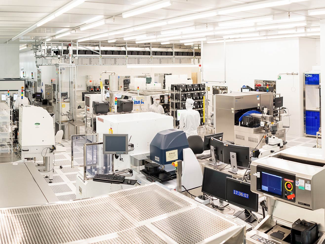
The Center Nanoelectronic Technologies (CNT) of Fraunhofer IPMS develops semiconductor technologies on 300 mm wafers and works on the integration of innovative functionalities into existing CMOS platforms. One focus is research on novel memory concepts and high-frequency devices based on ferroelectric CMOS-compatible materials. Furthermore, work is being carried out on energy-efficient power management systems that bring together solid-state batteries, harvesters and embedded capacitors. In addition, neuromorphic systems, technologies for quantum computing and spin-based devices are being researched. For its research, CNT uses a flexible modern toolpark and a wide range of manufacturing processes in a new industry-compatible clean room.
The CNT Screening Fab concept enables suppliers, equipment manufacturers and semiconductor companies to test new materials and manufacturing processes. "The services offered range from the qualification of manufacturing steps such as cleaning or etching, copper plating and CMP to the evaluation of new precursors for atomic layer deposition," summarizes Dr. Wenke Weinreich, head of the CNT division at Fraunhofer IPMS. In addition, CNT offers a wide range of methods for physical failure analysis and electrical characterization of semiconductor devices. CNT researchers will present examples from currently ongoing research and development work at the Fraunhofer IPMS booth at SEMICON Europa. These include embedded capacitors for miniaturized electronic systems. Test chips developed in‑house are available for the evaluation of CMP manufacturing processes.
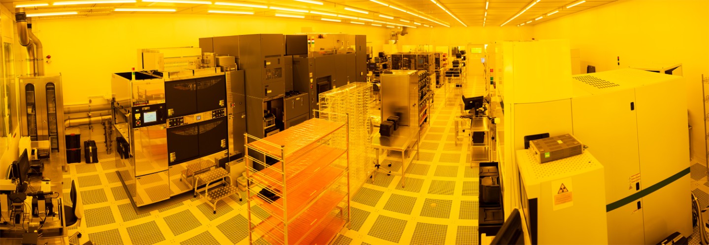
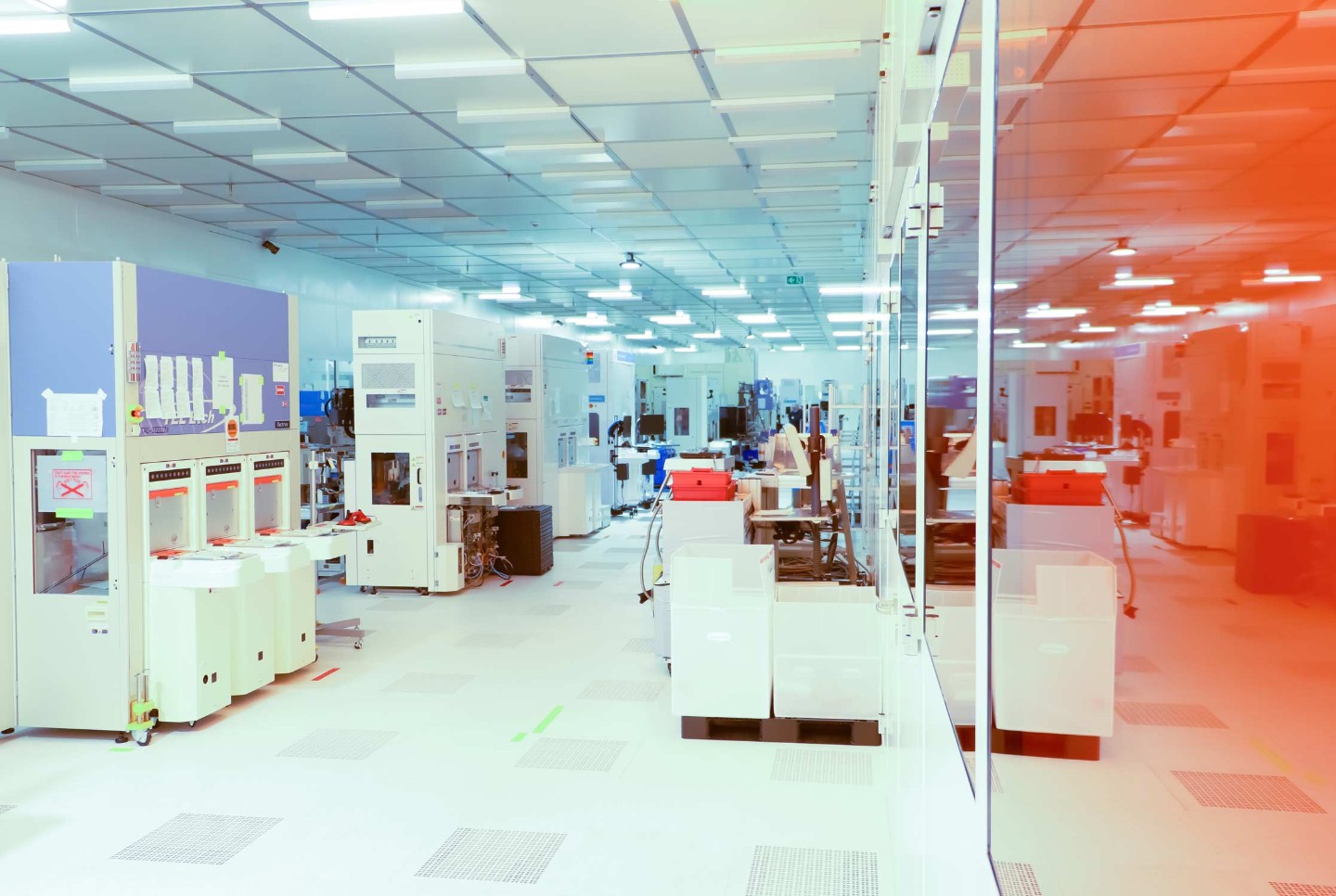
A second division of Fraunhofer IPMS, which is presenting itself at SEMICON Europa, offers its customers a complete service for the development of micro-electro-mechanical systems (MEMS) and micro-opto-electro-mechanical systems (MOEMS) on 200 mm wafers. These are manufactured in the institute's CMOS-compatible microsystems technology cleanroom. "The technological development and support of MEMS technologies, from individual process steps to technology modules to complete process flows, as well as the process-engineering support of the manufacturing equipment in the clean room, is ensured by our team," explains Thomas Zarbock, division director MEMS Engineering, Manufacturing & Test at Fraunhofer IPMS. "At customer's request, we take over pilot manufacturing after successful development or integration, or support a technology transfer to a foundry fab. With our business model in the MEMS area, Fraunhofer IPMS covers the Technology Readiness Levels (TRL) from three to eight," Zarbock continues.
At the booth at SEMICON Europa, the researchers of the 200 mm MEMS manufacturing of Fraunhofer IPMS will present highly sophisticated MEMS devices. These include spatial light modulators, which have recently been manufactured in the MEMS cleanroom using DUV lithography, among other methods, in order to enter the world of holography. For questions as well as a presentation of all services our experts are available at the fair.
You will find the Fraunhofer IPMS stall at the joint booth of the industry association Silicon Saxony (B.1221).
About Fraunhofer IPMS
The Fraunhofer Institute for Photonic Microsystems IPMS stands for applied research and development in the fields of intelligent industrial solutions, medical technology and improved quality of life. Our research focuses on miniaturized sensors and actuators, integrated circuits, wireless and wired data communication, and customized MEMS systems.