 Fraunhofer Institute for Photonic Microsystems
Chemical Mechanical Polishing (CMP)
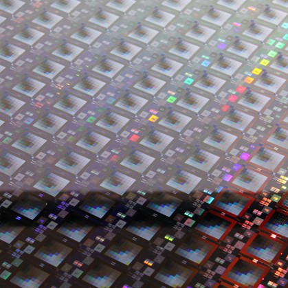
Highly integrated circuits, such as logic and memory chips, consist of many layers of material. In the course of production, the surfaces must be repeatedly planarised in order to obtain sufficient process windows for critical processes such as lithography and etching. Furthermore, planarisation ensures defined sizes of the structures and thus ultimately a reliable function of the electronic elements. Chemical-mechanical planarisation (CMP) is the state of the art to achieve the necessary planarity. The continuous miniaturisation in semiconductor technology is accompanied by a higher demand for accuracy as well as a higher number of materials used. Therefore, it is necessary to understand the different CMP processes and to develop new processes for newly introduced materials in order to meet the requirements of the upcoming technology nodes.
Fraunhofer IPMS offers:
- CMP process development and optimisation
- CMP design for the development of manufacturing strategies for and with semiconductor product manufacturers
- Screening and characterisation of CMP consumables (polishing pad - conditioner - slurry - post-CMP cleaning chemistry - brush - filter - and more)
- Characterisation of the CMP process (planarisation - defectivity - removal rates, selectivity - static etch rates - electrical performance and reliability)
- Modelling and simulation of the planarisation behaviour of structured wafers
- CMP wafer processing on request