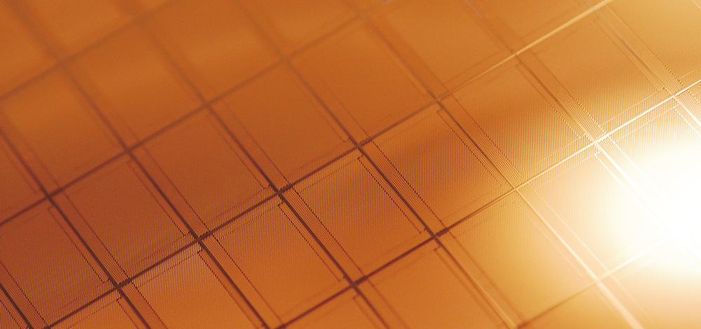
Wafer Metallization

The use of copper as a conductive material in the semiconductor industry revolutionised the metallisation process and was instrumental in enabling faster, smaller and less power consuming processors and integrated circuits. New process technologies enabled more complex and multi-layer interconnections, together with the electrical properties of copper, this led to a huge increase in the performance of processors.
At Fraunhofer IPMS, the ECD process and the copper material are constantly optimised to guarantee high performance and signal transmission with low energy requirements in combination with a long service life. To ensure this, the ECD process for the electrodeposition of metal layers is investigated by electrolyte screening, bath life investigation and process characterisation. Electrochemical measurement techniques and extensive analysis are available to study copper superfillings.
Our application areas
- 28 nm technology nodes and below
- 300 mm/12 in wafer & beaker tests
- Dual damascene plating
- Bump plating
- TSV plating
 Fraunhofer Institute for Photonic Microsystems