Fraunhofer Institute for Photonic Microsystems
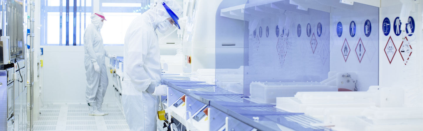

Research and development offer
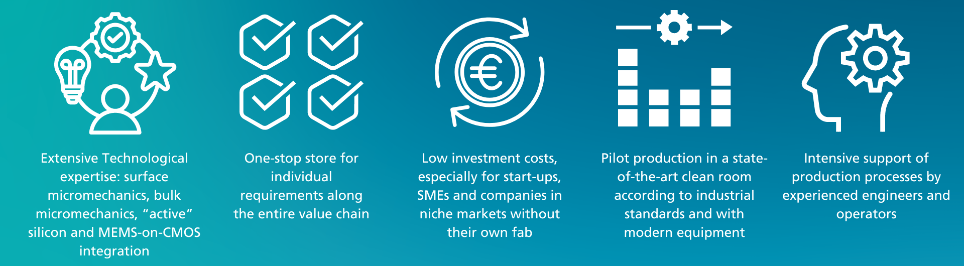
We offer you the complete service for the development of micro-electro-mechanical systems (MEMS) and micro-opto-electro-mechanical systems (MOEMS) on 200 mm wafers.
The technological development and support of MEMS technologies, from individual processes to technology modules to complete technology, as well as the process-related support of the systems in the clean room, is provided by our team of over 90 engineers, operators and technicians. On request, we take over pilot manufacturing after successful development or support a technology transfer. We cover the technological maturity levels (TRL) from three to eight.
Our offer at a glance
- Low volume & high mix
- 24/5 - 3 shift operation
- 45 engineers + 45 operators and maintenance technicians
- ~1,000 wafer starts per month
- CMOS compatibility
- Class 10 (ISO 4) on 1,500 m²
- ISO 9001:2015 certification
- MES for planning, traceability and documentation
- i-line (400nm L&S) and DUV cluster (130nm L&S)