30 years of Fraunhofer in Dresden

30 Jahre Fraunhofer in Dresden – 30 Jahre Fraunhofer IPMS

In 2022, the Fraunhofer-Gesellschaft celebrated its 30th anniversary in Dresden. The Fraunhofer IPMS started as a branch of the Fraunhofer IMS Duisburg and became an independent institute in 2003. From 150 employees and a budget of €13 million, it has now grown to more than 500 employees and a budget of over €50 million. Have a look back with us at 30 successful years!

1992: Foundation of Fraunhofer IMS with location in Dresden

Location of the Fraunhofer IMS (later IPMS) at Mara-Reiche-Straße 2 in Dresden.

Starting from the Center for Microelectronics Dresden and the institutes of the Academy of Sciences, two Fraunhofer facilities in the field of microelectronics were founded in 1992 after intensive preparations in Dresden. One of them was the Institute for Microelectronic Circuits and Systems located in Duisburg and Dresden, which later became Fraunhofer IPMS. It worked in the fields of CMOS technology, sensor technology, analog and digital circuits, and system development.

2003: Fraunhofer IMS in Dresden becomes a separate institute named Fraunhofer IPMS

© Stadtkind360
Aerial view of Fraunhofer IPMS with office buildings and 200 mm MEMS cleanroom.

The Fraunhofer IMS Dresden becomes a separate institute - the Fraunhofer Institute for Photonic Microsystems IPMS. With about 150 employees and a budget of about € 13 million, the institute started under the direction of Prof. Dr. Hubert Lakner. He is still the institute director at Fraunhofer IPMS, today together with the managing director Prof. Dr. Harald Schenk. The institute has grown significantly in the process: It now has around 500 employees at four locations with an annual budget of approximately €50 million.

2007: Clean room inauguration in Maria-Reiche-Straße

200 mm MEMS clean room at Mara-Reiche-Straße 2 in Dresden.

In 2007, the construction measures for the expansion and modernization of the Fraunhofer IPMS were completed after a two-year construction period. On September 10, 2007, Fraunhofer IPMS celebrated the inauguration of the renovated institute building and the new clean room. The new clean room laid the foundation for many successful developments of Fraunhofer IMPS, for example microscanning mirrors or area light modulators.

2011: Construction of the "Fraunhofer Bridge" between the buildings

Übergang an der Mara-Reiche-Straße.

Due to growth, the Fraunhofer IPMS needed more space and additionally received part of the left section of the building Maria-Reiche-Straße 5 as an extension. In 2011, the energetic renovation and modernization took place. To ensure accessibility to the extension building, a transition in the form of a bridge was created starting from the institute building. And since last year it is also wonderfully illuminated!

2013: Center Nanoelectronic Technologies becomes part of Fraunhofer IPMS

Location of the Center Nanoelectronic Technologies at Wilschdorfer Landstraße in Dresden.

The Fraunhofer Center Nanoelectronic Technologies became a business unit of the Fraunhofer IPMS in 2013. Started in 2006 with 6 employees, it already had over 50 in 2013! With its 800 m² clean room at Königsbrücker Straße, it had an excellent infrastructure for process and material development on 300 mm wafers. Since 2021, the CNT has a new location "An der Bartlake 5". 90 people now work in this business unit and in a now 3000 m² cleanroom.

2015: Foundation of Performance Center Micro/Nano

Opening ceremony of the "Functional Integration for Micro-/Nanoelectronics" performance center.

In 2015, the Fraunhofer Institutes IPMS, ENAS, IIS and IZM joined forces with the Technical Universities of Dresden and Chemnitz and the Dresden University of Applied Sciences to form the "Functional Integration for Micro- / Nanoelectronics" performance center. In close cooperation with local companies, research know-how is to be deepened, innovations are to be implemented more quickly in applications and products, and the region is thus to be strengthened.

2016: Changeover of the MEMS clean room from 150 to 200 mm

Ceremonial changeover of the MEMS clean room to 200 mm.

On September 21, 2016, Fraunhofer IPMS celebrated the conversion from 150 mm wafer substrates to a 200 mm process line in its MEMS clean room. The most important research and development partners had already switched to 200 mm wafer technology at that time. The upgrade to the 200 mm wafer format was therefore a prerequisite for continuing to work with industry partners at the top level to which we are accustomed. The existing supply infrastructure was adapted, existing equipment and processes were converted, and new equipment was procured and installed.

2017: Foundation of the Research Factory Microelectronics Germany (FMD)

Opening of the Research Factory Microelectronics Germany (FMD) in Dresden.

On August 8, 2017, Fraunhofer IPMS celebrated the launch of the Research Factory Microelectronics Germany (FMD). The eleven institutes of the Fraunhofer Group for Microelectronics together with the Leibniz Institute for Innovative Microelectronics IHP in Frankfurt/Oder and the Berlin Ferdinand-Braun-Institut, Leibniz-Institut für Höchstfrequenztechnik FBH work together in the FMD. The FMD contributes significantly to the technological sovereignty of Germany and Europe and allows the institutes to invest in state-of-the-art, high-performance facilities, laboratory and instrumentation equipment and thus offer internationally outstanding research services.

2018: Founding of the Integrated Silicon Systems (ISS) part of the institute in Cottbus.

Opening of the ISS part of the institute in Cottbus.

On April 19, 2018, Fraunhofer IPMS ceremoniously opened its new institute section "Integrated Silicon Systems" at the central campus of BTU Cottbus-Senftenberg. The institute's director Prof. Harald Schenk, holder of the professorship Micro and Nano Systems at BTU Cottbus-Senftenberg, had initiated the collaboration between BTU Cottbus-Senftenberg and Fraunhofer IPMS with the establishment of the project group "Mesoscopic Actuators and Systems" (MESYS) on site in Cottbus in 2012.

Research is being conducted on electrostatic microactuators - so-called nanoscopic electrostatic drives (NED). The new class of actuators, which has already been patented, is CMOS-compatible and solves fundamental problems of electrostatic actuators. Possible application fields are MEMS loudspeakers or micropositioning systems.

2018: Founding of the Fraunhofer Center for Microelectronic and Optical Systems for Biomedicine (MEOS) in Erfurt.

Opening of the Fraunhofer Center MEOS in Erfurt.

Detecting and treating diseases in time with the help of optical microsystems - this is the goal of the "Fraunhofer Center Microelectronic and Optical Systems for Biomedicine" (MEOS) at the Erfurt site, which was officially opened on October 19, 2018. In the center, Fraunhofer IMPS collaborates with Fraunhofer IZI and Fraunhofer IOF. MEOS focuses on work on structured illumination in microscopy, medical optical imaging, and technologies for biomarker analysis.

The interdisciplinary approach of linking life sciences, microelectronics as well as optics and photonics shall lead to the successful further development of biomedical applications and to new medical engineering solutions.

2021: Relocation of the Center Nanoelectronic Technologies to a new location

Location of the Center Nanoelectronic Technologies at Wilschdorfer Landstraße in Dresden.

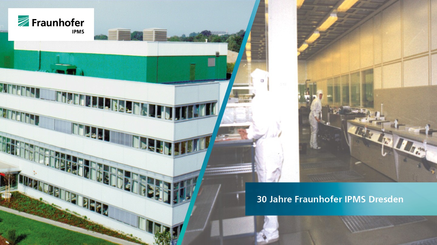
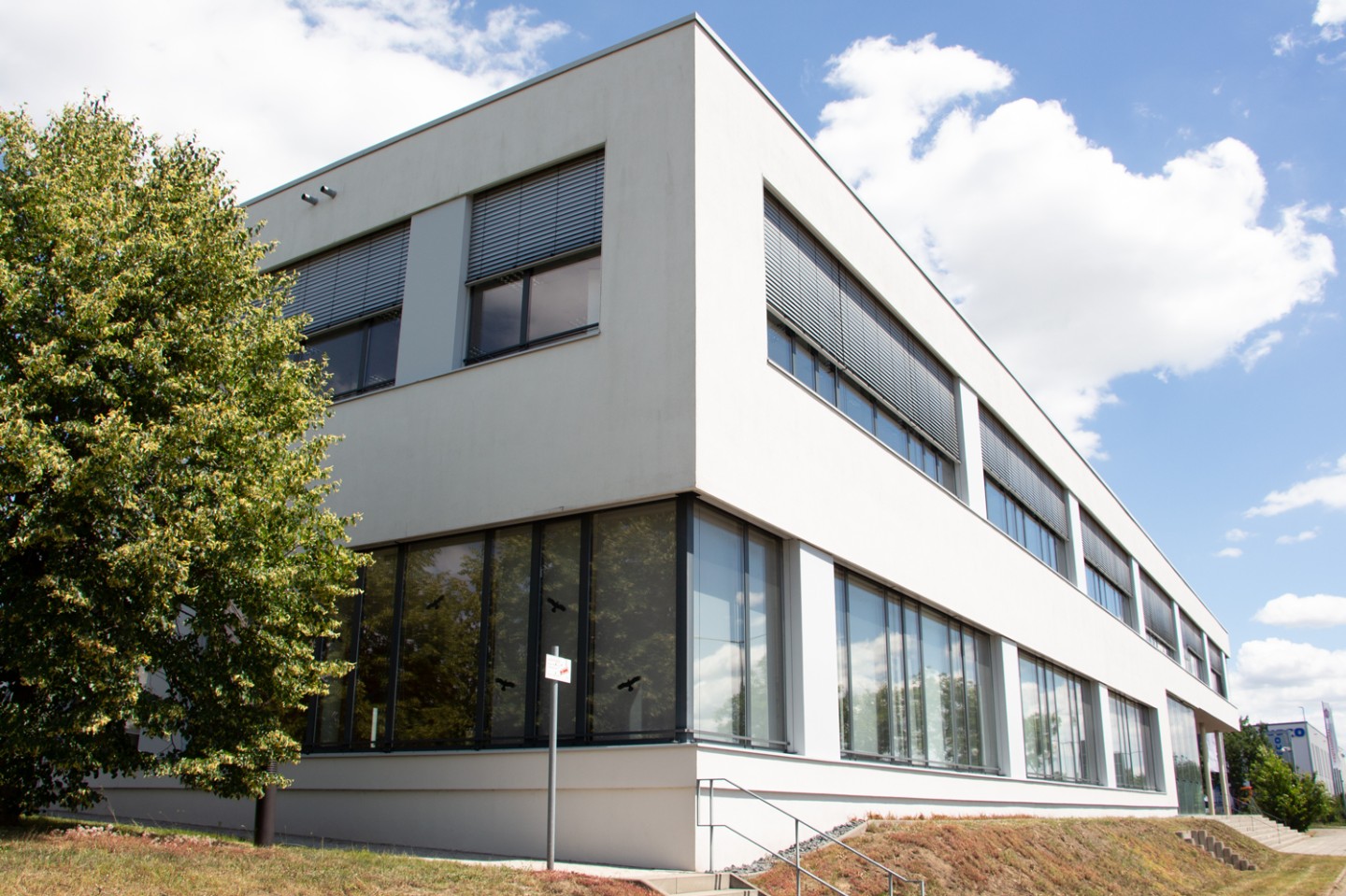
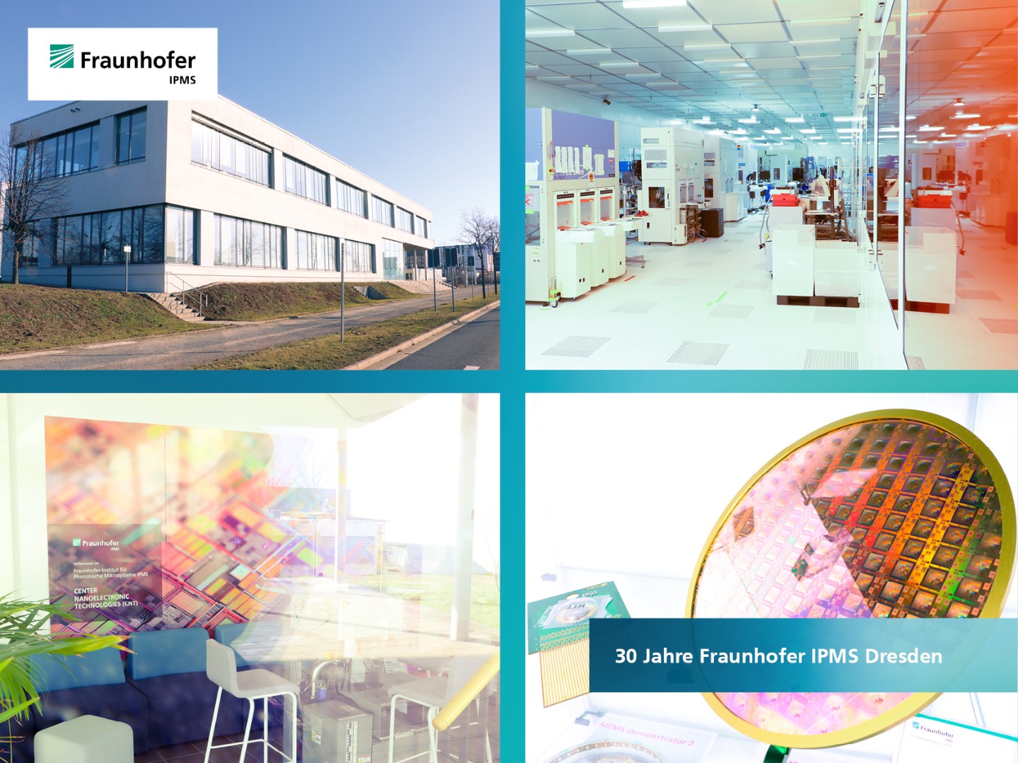
With the Center Nanoelectronic Technologies CNT, Fraunhofer IPMS conducts applied microelectronics research on 300 mm wafers for microchip producers, suppliers, equipment manufacturers and R&D partners. Previously, 800 m² of clean room space at Infineon Technologies Dresden GmbH on Königsbrücker Landstraße was used for this purpose. Due to strong economic demand, our long-standing partner now needed the space itself to expand its production capacities. Thanks to the very good support of the Free State of Saxony and the headquarters of the Fraunhofer-Gesellschaft, it was possible to jointly find a new home for the CNT.

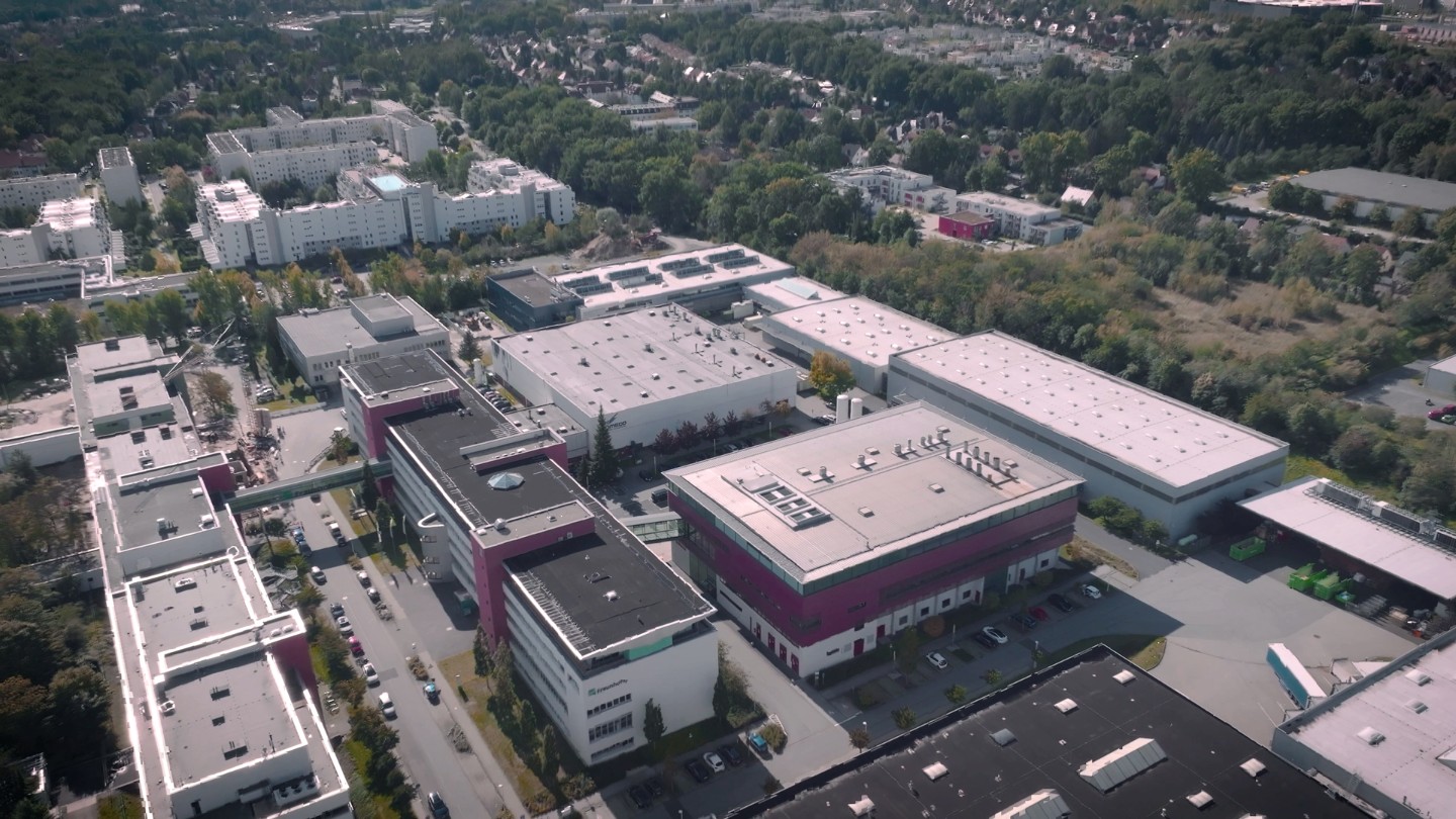
The move to the new location in the north of Dresden began in early 2021. Until then, a structural adaptation to the requirements of the CNT took place. With now 4000 m² clean room space, the new location offers not only optimal conditions for the continuation of the 300 mm research activities, but furthermore the potential for further growth. In the next construction phase, a new office building will be erected.

2022: Opening of the Center for Advanced CMOS & Heterointegration Saxony

© Schneider-Bröcker
Opening of the Center for Advanced CMOS & Heterointegration Saxony at the CNT site on Wilschdorfer Landstraße.

At the beginning of June, Dresden celebrated a beacon of semiconductor research with international reach. With the establishment of the "Center for Advanced CMOS & Heterointegration Saxony", the Fraunhofer IPMS and the Fraunhofer IZM-ASSID bundle their competences. In the future, they will offer the complete value chain in 300 mm microelectronics and thus the prerequisite for high-tech research for future technologies.

With the Fraunhofer IZM-ASSID and Fraunhofer IPMS, area Center Nanoelectronic Technologies CNT, two unique research facilities in Germany in the field of microelectronics are located in Saxony. Today, they are the only two German research centers for applied microelectronics research based on 300 mm wafer industry standard equipment.

2022 and in the future

We research for the applications of tomorrow. We are courageously continuing on our successful path. We would be pleased to inform you about our strategic research fields.