 Fraunhofer Institute for Photonic Microsystems
Photonics West 2012
San Francisco, USA, January 24 - 26, 2012, Booth 4417
Liquid crystals waveguide switching technology
At the Photonics West 2012 show in San Francisco from 24th to 26th January 2012 the Fraunhofer Institute for Photonic Microsystems IPMS presents a novel optical liquid crystal switch.
Either for signal switching in optical communication networks or fiber sensor networks the optical path connection needs to be dynamically controlled. Optical switches and routers are devices designed to execute such essential control functions.
The market makes demands on current optical switching device technologies for high reliability and stability of switching, for switching between many input- and output-channels as well as for providing low optical loss, low cross-talk and short switching times.
Optical switches with no moving parts, such as the liquid crystal based devices, warrant high operation stability and reliability. This is one of the reasons to decide for Fraunhofer IPMS's liquid crystal optical switching devices. Yet, what makes this technology truly attractive is the use of isotropic liquid crystals which, through the underlying quadratic electro-optic Kerr effect, render the device remarkable properties: sub-micro-second switching times and excellent transparency over a broad spectral range from 400 nm to 1600 nm, at a still reasonable operation voltage. All the more, due to their straightforward design, these devices are easily integrable and manufacturable by means of high precision, planar silicon wafer technology.
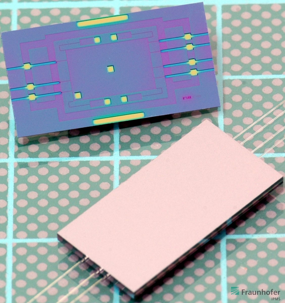
The Fraunhofer IPMS's optical switching device, presented in the figure, is made on two bonded silicon wafers – forming the base and the top parts of the chip – each including structured electrodes stripes. The wafers enclose in between an isotropic liquid crystal layer. An electric field applied between selected electrodes from both parts of the chip and across the liquid crystal layer causes a local change of the refractive index on corresponding regions inside this layer. Light waves can be guided on the paths, thus ›activated‹, at an optical loss of better than 2 dB/cm.
The technology based on such ›active‹ optical waveguides permits, just by structuring suitable electrodes on the chip, the fabrication of optical switches with multiple inputs and outputs at either single- or multi-mode operation.
Fraunhofer IPMS's optical switching device technology offers hence remarkable advantages in terms of switching stability and reliability, since no moving parts are involved, then device design flexibility and scalability are warranted as well as simple wafer level fabrication. The requirements for low cost and high volume manufacturing are therefore met. Furthermore, by using this technology, the range of functions implemented on a device can be extended to include interconnection, optical attenuation and modulation. These devices can be tailored to meet the specific needs of optical networks, remote sensing and laser technology applications.
About Fraunhofer IPMS
The Fraunhofer Institute for Photonic Microsystems IPMS and its 220 employees turn over an annual research volume of nearly 26 million euros. Fraunhofer IPMS generates more than two thirds of this production capacity out of commissions from industry and publicly financed projects in applied research. The focus of our development and production services lies in the practical industrial application of unique technologicalknow-how in the fields of (optical) micro-electromechanical systems [MEMS, MOEMS]. Fraunhofer IMPS uses scientific know-how, application experience and customer contacts as well as modern equipment and clean room infrastructure. Fraunhofer IPMS covers a broad spectrum of industrial applications. Our services range from initial conception toproduct development, right down to serial pilot production – from a single component to a complete system solution.