200 mm MEMS Cleanroom

Research and development offer

Fraunhofer IPMS offers its customers the complete service for the development of micro-electro-mechanical systems (MEMS) and micro-opto-electro-mechanical systems (MOEMS) on 200 mm wafers. The technological development and support of MEMS technologies, from individual processes to technology modules to complete technology, as well as the process-related support of the systems in the clean room, is provided by our team of over 90 engineers, operators and technicians. On customer request, we take over the pilot manufacturing after the successful development or support a technology transfer, whereby the Fraunhofer IPMS covers the technological maturity levels (TRL) from three to eight.

Our advantages and features at a glance

Advantages

  • Extensive technological competence in the field of surface micromechanics, bulk micromechanics, "active" silicon as well as MEMS-on-CMOS integration
  • One-stop store for individual requirements along the entire value chain
  • Low investment costs especially for start-ups, SMEs and companies in niche markets without own fab
  • Pilot production in a state-of-the-art clean room according to industrial standards and modern equipment park
  • Intensive support of the manufacturing processes by experienced engineers and operators
  • DUV lithography cluster with which structures of 130 nm L&S can be realized
Features
  • Low volume & high mix
  • 24/5 - 3 shift operation
  • 45 engineers + 45 operators and maintenance technicians
  • i-line (400nm L&S) and DUV cluster (130nm L&S)
  • ~1,000 wafer starts per month
  • CMOS compatibility
  • Class 10 (ISO 4) on 1,500 m²
  • ISO 9001:2015 certification
  • MES for planning, traceability and documentation

Our MEMS Technologies

In addition to the conceptual design, development and fabrication of MEMS and MOEMS devices, Fraunhofer IPMS possesses the know-how for the fabrication of individualized BSOI wafers, the electrical characterization of devices and develops suitable packaging solutions following fabrication.

MEMS Technology Analysis - Electrical Characterization

© Fraunhofer IPMS
Characterization at wafer level

To characterize the complex devices and technologies, Fraunhofer IPMS is able to perform the following measurements (in-/ex-situ) both at wafer level and on the individual device:

  • Mixed-signal testing
  • Parametric test system
  • Electro-optical test system for micro-displays and sensors
  • Sensor-actuator test system
  • Non-electrical test
  • Optical inspection
  • CV analysis
  • Insulator integrity and reliability characterization
  • More: MEMS/MOEMS Process Developments and Tool Park

Wafer Bonding

© Fraunhofer IPMS
Pick and place of a spatial light modulator (SLM)

Wafers can be thinned for the manufacturing of BSOI wafers by means of CMOS-compatible grinders. Furthermore, Fraunhofer IPMS recently enhances BSOI wafers with novel features, such as cavities, buried guideways or even multi-SOI structures.

Further bonding capabilities are:

Packaging and Assembly

© Fraunhofer IPMS

MEMS devices open up new possibilities in the miniaturization of systems. Fraunhofer IPMS offers corresponding development services to help our customers create innovative products. However, the system design using MEMS, electronics, optics and other photonic components and the processes for assembling the systems in the smallest volumes are mutually dependent. Fraunhofer IPMS therefore has the necessary expertise and equipment for microassembly and also offers small batch manufacturing as a service.

System development and small batch manufacturing:

  • System development and system realization from one source
  • Realization of two- and multi-component superstructures
  • Realization of 2D and 3D superstructures
  • More: Back End and Packaging

IC Design

IC Design at Fraunhofer IPMS

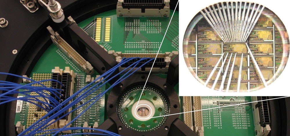
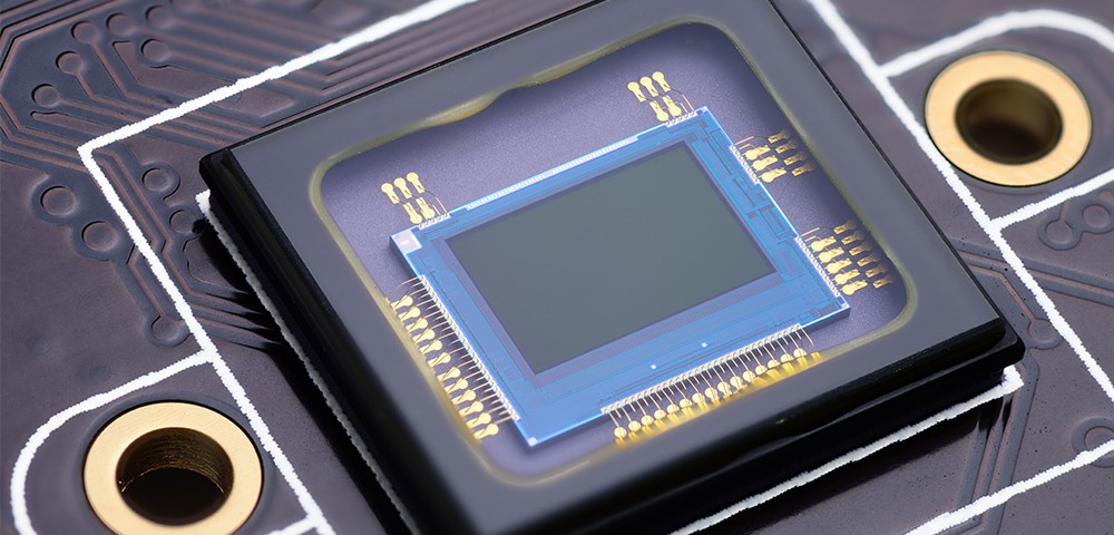
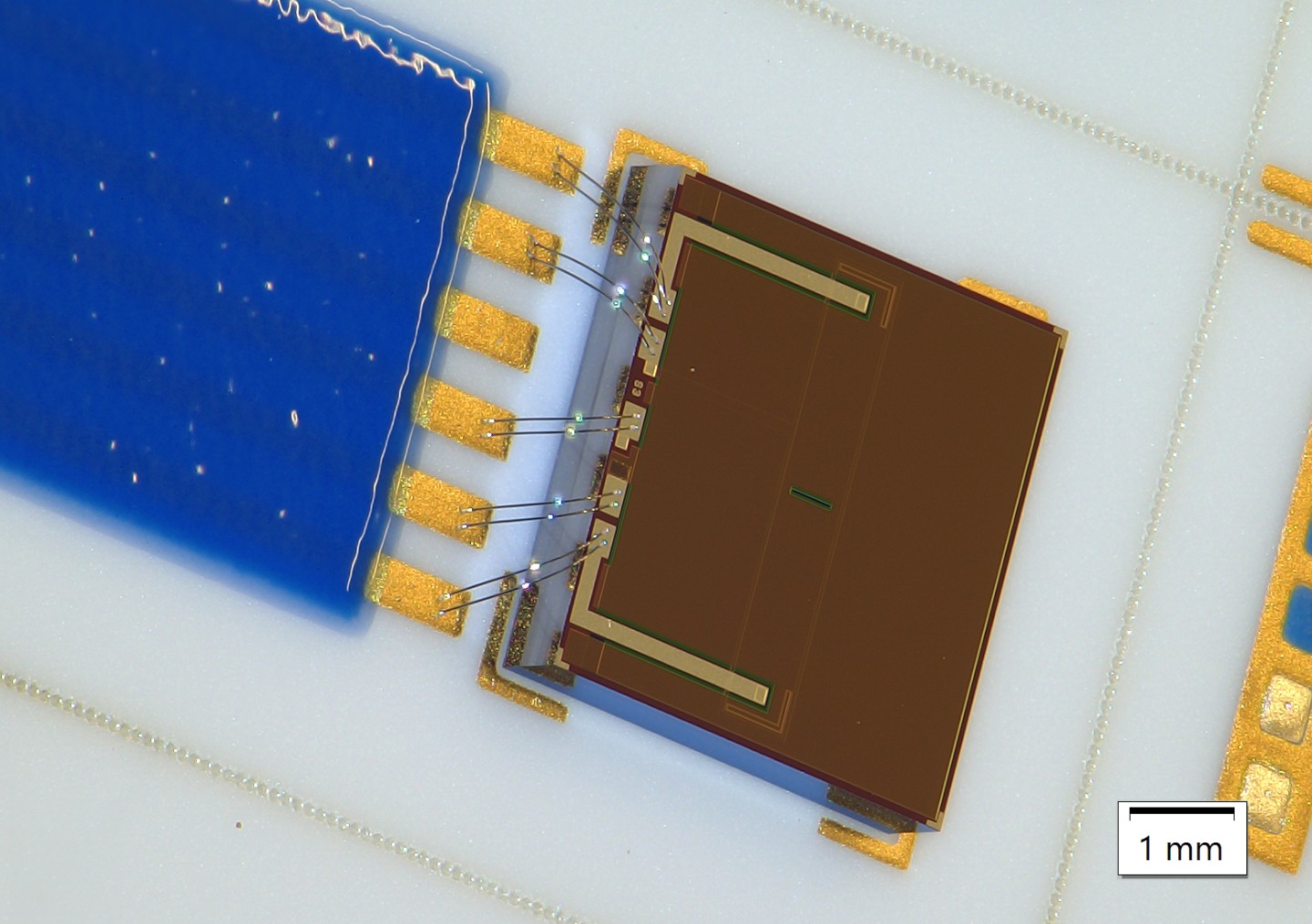
The design of application-specific integrated circuits facilitates creation of highly complex microelectronic devices such as microdisplays and optoelectronic sensors. The methodology of this design process is based around circuit simulation, layout design, and verification. We create these kinds of designs using industry-standard software tools and implement them in mixed analog/digital CMOS processes in partnership with silicon circuit foundries worldwide. Following fabrication of the circuits in silicon, the functionality is verified by means of wafer-level and component-level testing, then prototypes are created. Transfer to pilot production can then take place on a project-specific basis.

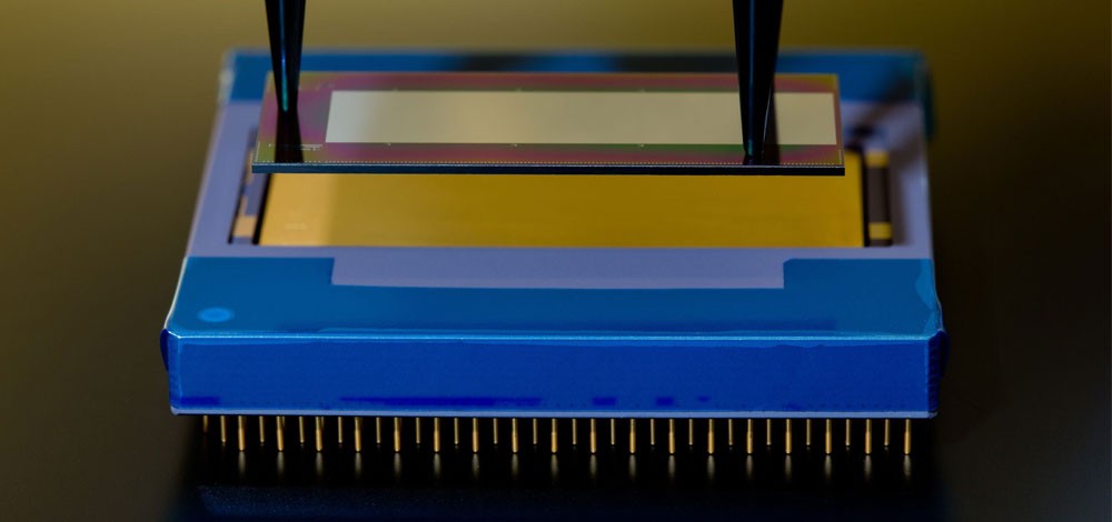
The Fraunhofer IPMS has a unique position in designing microelectronic circuits and components with application- and customer-specific adaptations of silicon circuit foundries’ CMOS processes that allow these finished wafers to be subsequently processed with OLED coatings, for example. This subsequent processing is used in particular for augmenting silicon CMOS wafer functionality with optical and photonic components, such as for high-resolution OLED microdisplays

  • Design of microelectronic circuits and modules through application-specific adaptation of CMOS processes
  • Industry-compatible circuit simulation, layout design, and verification
  • Implementation in mixed analog/digital CMOS processes of silicon circuit foundries
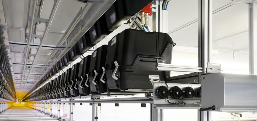
  • Prototype fabrication, transfer to pilot production

Intelligent BSOI wafers

© Fraunhofer IPMS
BSOI wafers according to customer requirements

The increasing demand for BSOI wafers, coupled with the requirements for our sophisticated components, have led Fraunhofer IPMS to build up competencies in the field of BSOI manufacturing in recent years. In doing so, our approach addresses individualized solutions for our customers in BSOI wafer fabrication. The devicelayers are equipped with various features, such as an adapted layer thickness and adapted doping. Thanks to our many years of technological experience, add-ons such as cavities or buried conductor paths can also be integrated into the device layer. This enables our customers to make optimum use of resources and short process times in the development of sophisticated products. The necessary technology modules are available to us and are completed by the following capabilities:

Surface Micromechanics

© Fraunhofer IPMS
Principle of surface micromechanics

Using sacrificial layer technology, Fraunhofer IPMS is able to manufacture actuators and sensors such as surface light modulators (SLM) and capacitive ultrasonic sensors (CMUT). The processes and technology modules available to Fraunhofer IPMS for these highly complex components are:

  • PE-CVD for TEOS, HDP and a:Si.
  • Five-zone CMP for high planarity
  • Anti-stiction for excellent reliability
  • PVD for joints and mirrors with stress tuning
  • ALD for barrier coatings
  • Gas phase etching using HF and XeF2 for sacrificial layer processing
  • More: MEMS/MOEMS Process Developments and Tool Park

Volume Micromechanics

Principle of volume micromechanics
© Fraunhofer IPMS
Principle of volume micromechanics

Whether high-precision mirrors or the unique Nano-E-Drive principle developed by Fraunhofer IPMS: these actuators are based on deeply etched silicon structures with large aspect ratios (up to 40). In addition to the competencies in surface micromechanics, the following modules are available for further development:

  • Grinder for wafer thinning
  • PVD for highly reflective layers
  • Wafer bonding for quasi-static motion
  • Deep silicon etching for the realization of comb drives
  • TMAH etching for backside openings
  • Trench backfill for insulation
  • B-SOI wafers as starting materials
  • More: Mechanical Actuators

Monolithic MEMS-on-CMOS Integration

Integration of MEMS on CMOS

Monolithic integration of MEMS on CMOS is an integration technology for the fabrication of wafer-level integrated systems. Fraunhofer IPMS develops and manufactures monolithically integrated MEMS to minimize parasitic effects. With this technology, especially large devices with a high integration density can be realized reliably. Examples are SLMs, thermopile and CMUT arrays.

Active Silicon

© Fraunhofer IPMS
Ion-sensitive field-effect transistor of the Fraunhofer IPMS

Fraunhofer IPMS manufactures wafer-level components that utilize the chemical and physical properties of functional layers, e.g. in ion-sensitive field-effect transistors (ISFET) for measuring pH values.

  • Thermal oxidation for gate oxides (SiO2)
  • Deposition of active layers (e.g. Nb2O5)
  • More: Chemical Sensors

Virtual tour of our 200 mm MEMS cleanroom

MEMS Applications

Fraunhofer Group for Microelectronics

Towards technology sovereignty.