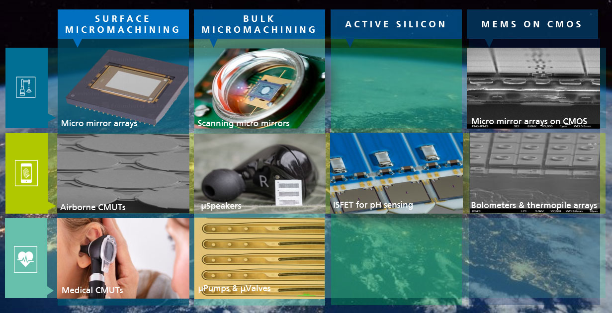
The Fraunhofer IPMS cleanroom is ideally positioned for research and development in the field of MEMS and MOEMS devices with its qualified team and industry-oriented facilities. In addition to the in-depth understanding of leading edge MEMS manufacturing processes, coupled with modern fab technology, we are the perfect partner for the development of technologies and devices.
MEMS Applications
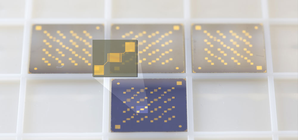
End-of-line substrates for characterization of organic semiconductor materials
For some years now, organic electronics has been regarded as the key term for a new type of application realized on the basis of organic semiconductors and other easy-to-process materials. Typical of this new class of materials are low-temperature processes and large-area deposition and structuring using a wide variety of coating and printing processes. The active semiconductor materials essentially determine the performance of the overall system. Therefore, a simple and reliable electronic characterization of these semiconductors is an indispensable requirement not only for material development in the laboratories of organic chemists, but also for process developers and circuit designers.
For material analysis in the field of organic semiconductors, Fraunhofer IPMS provides standardized single transistor structures in bottom-gate architecture. These substrates for organic field-effect transistors (OFET) are fabricated on silicon wafers with thermal silicon dioxide (SiO2) as full-area dielectric and gold electrodes in lift-off technology in the Fraunhofer IPMS clean room.
Thermopile arrays
For the fabrication of thermopile arrays, we have maintained a close partnership with the leading manufacturer Heimann Sensor for over 10 years. Thermopile arrays are used especially in times of Corona for the detection of radiated body temperature. This is used, for example, at airports for the early detection of infectious air travelers.
In cooperation, the thermopile arrays are being iteratively developed and manufactured at IPMS. The three partners, consisting of Heimann Sensor as the product developer, XFAB as the CMOS supplier and the IPMS as the technology partner for the back-end area, are currently working on a project that will lead to a further improvement in pixel size and, as a direct consequence, to a higher pixel density while maintaining the same array size, thus optimizing the resolution. The IPMS is primarily responsible for the hard mask, the isolation structures and the absorber structures and transfers these components for final processing to Heimann Sensor for the realization of pixel arrays with resolutions up to 120x84. The fabrication of existing component generations takes place continuously.
Photodiode
The fabrication of photodiodes has a long tradition at IPMS and has been optimized over a long period of time.
In the process, we have always made customer-specific adjustments:
- Parameters of the diodes (high sensitivity (NIR), high cut-off frequency, low dark current).
- MST components (pit for covering / contacting the LED)
- Backside photodiode
The silicon photodiodes reach the maximum sensitivity at l = 0.8 to 0.9 µm.
Micro mirror arrays as programmable mask
The development of the micromirror arrays as programmable masks for mask exposure systems is carried out at Fraunhofer IPMS on behalf of Mycronic, Sweden. In addition to the further development of the products, the focus is on the small series delivery of qualified components. These qualified components comprise 1 million tilting mirrors with single mirror dimensions of 16 µm × 16 µm, the frame rate is 2 kHz. The components are used in high-resolution mask writers of the SIGMA series from Mycronic
In parallel to the delivery activities, Fraunhofer IPMS is working on the development of mirror technologies for future applications with even higher device requirements. Wafer bonding technologies have been successfully investigated which allow to use also single crystalline silicon as actuator material. The mechanical properties of this material significantly exceed those of currently used aluminum alloys. Furthermore, first demonstrator devices equipped with Si mirrors show promising mirror planarities. One of the greatest challenges of this new technology is to bring the necessary technological processes to fabrication readiness. Here, the considerable chip dimensions of 15 mm × 38 mm in combination with the complex wafer bonding processes have to be taken into account.
Microdisplays and Sensors
We offer technology and process development for organic electronic components on our pilot production lines, from layout development to encapsulation and component integration for OLEDs, microdisplays, and sensors.
Our core expertise in organic electronics includes the development of technologies and processes for the fabrication of organic electronic components based on semiconducting hydrocarbon compounds. Pilot production lines are available for this purpose. Our focus is on process development for the deposition and structuring of thin organic layers as well as on encapsulation and system integration. The portfolio ranges from the creation of simple OLED layouts on various substrates up to OLED-on-silicon technologies (e.g. for microdisplays) and component integration. The components are used in OLED-microdisplays, in organic photodiodes for sensors, organic photovoltaics (OPV) and organic thin-film transistors.
Our offer
- Technology and process development for organic electronic components on research and pilot production lines
- We cover the complete value chain – from developing the layout to final encapsulation
- Module integration for OLEDs, microdisplays, and sensors
- Inspection and sample production
- Evaluation and characterization of the devices
- More information about Organic Light Emitting Diode (OLED)
 Fraunhofer Institute for Photonic Microsystems


