Fraunhofer Institute for Photonic Microsystems
In today's standard transistor production, the individual devices are electrically separated from each other by purposefully produced deep trenches of insulating silicon oxide. In order to adjust the dimension of the isolation trenches to nanometer accuracy, a chemical mechanical planarization (CMP) process is required. Today, this step uses a polishing suspension (slurry) based on cerium oxide abrasive particles. Since cerium is a rare earth element whose oxide is suspected of being carcinogenic, tests are underway at Fraunhofer IPMS with more environmentally compatible alternative slurries based on silicon oxide.
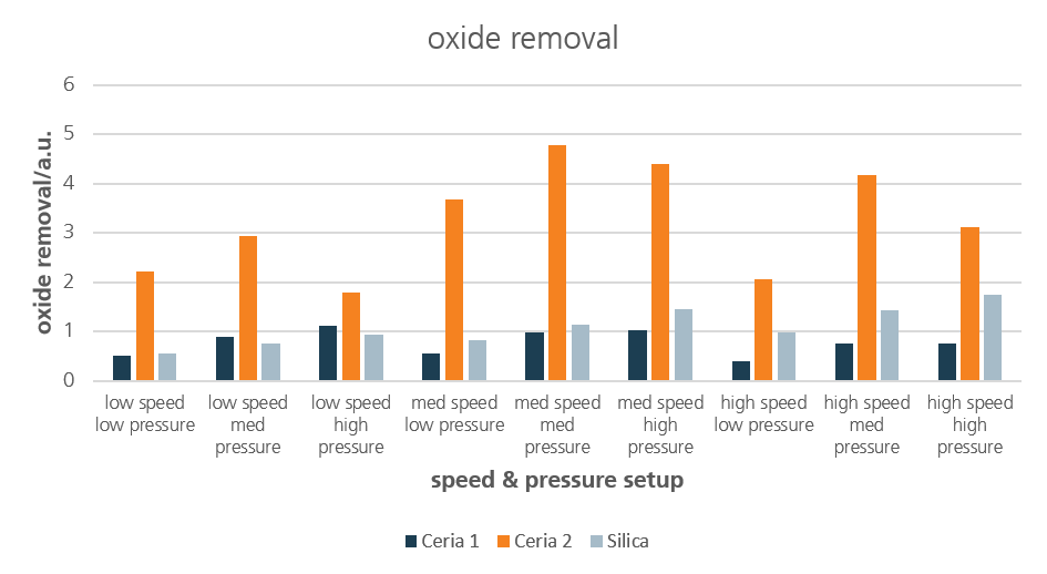
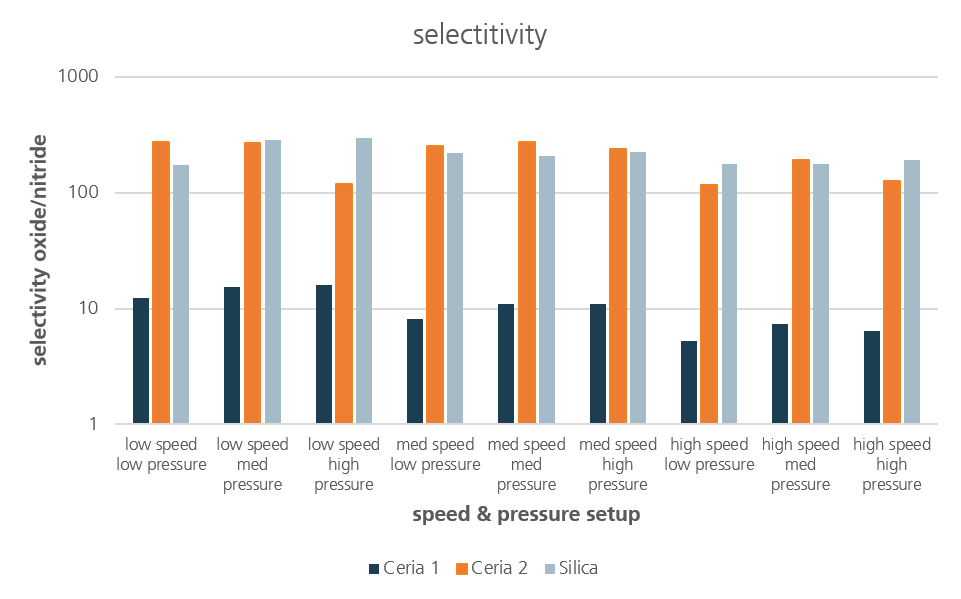
Since silicon oxide is removed during the manufacturing process and the topography is adjusted with the help of a polishing stop layer made of silicon nitride, (at least) two parameters are of central importance for evaluating a slurry: the oxide removal should be sufficiently high to enable a high process throughput. A high selectivity of the removal is required to stop the process when the polishing stop layer is reached.
The comparison of the oxide removal of two ceride and one silica slurry can be seen in the following diagram: