 Fraunhofer Institute for Photonic Microsystems
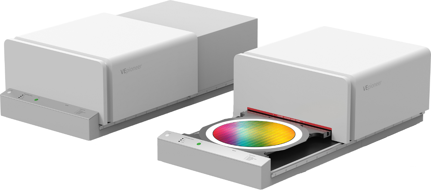
Together with DIVE imaging systems GmbH we are working on a joint project within the GreenICT Space - the accelerator program of the competence center "GreenICT@FMD".
The overarching aim of the project idea is to establish hyperspectral vision technology as a production-accompanying screening tool for semiconductor production. The aim is to make the semiconductor production chain more efficient and therefore more environmentally sustainable.
For example, based on the information collected, previously required system control wafers can be saved to a significant extent, faulty production can be recognised earlier and subsequently avoided, new (wafer) designs can be established more efficiently and production capacities can be optimised and utilised in a more resource-efficient manner overall.
This significantly reduces the consumption of materials, energy and consumables per wafer in semiconductor production. considerably.