Fraunhofer Institute for Photonic Microsystems
Organic field-effect transistor (OFET) – Substrates for Material Characterization
Diced OFET substrates from Fraunhofer IPMS.
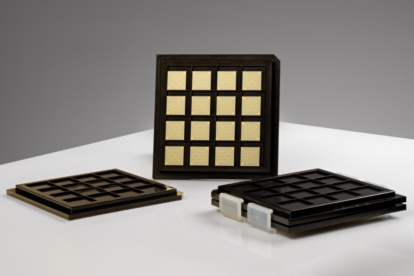
OFET substrates from Fraunhofer IPMS in a waffle pack.
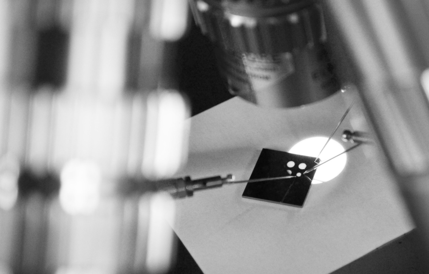
OFET measurement setup example.
We offer a wide range of services and chemical sensors for industry and science
- Standard and customized OFET substrates for your organic materials
- Measuring adapter and deposition masks/shadow masks
- Waffle pack and wafer size (diced)
- Industrial technology supplier
- OFET RnD Expertise for over 10 years
- Testing and Application partner
For Semiconductors and conductors we offer highly reproducible measurements of:
- Conductivity
- Carrier mobility
- On/Off current ratio
- Influence of annealing and solvent
- Determination of contact resistance
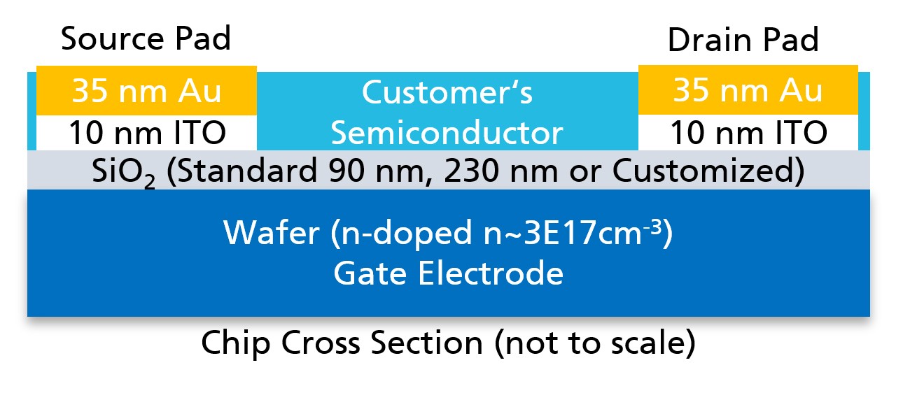
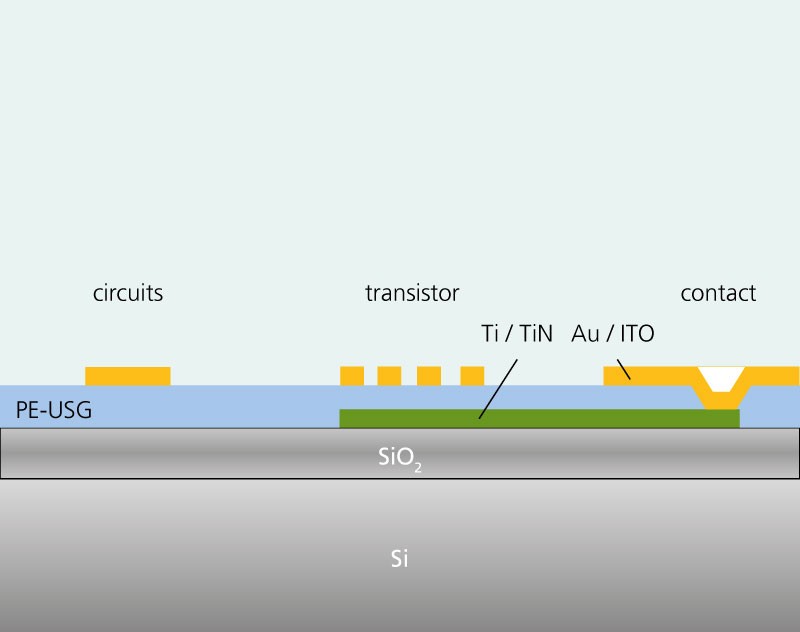
Example OFET substrate design
- n-doped and backgated OFET substrates
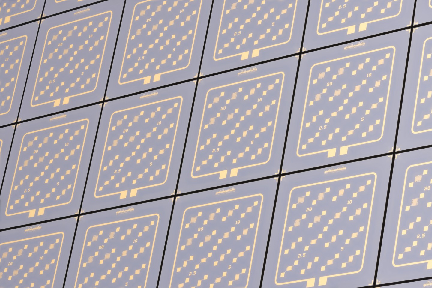
- 16 transistors per chip with different channel sizes
- large channel width (W = 2.5 ... 20 µm, L = 10 mm)
- High reproducibility
- Gate oxide starting at 28 nm for low voltage