Analytics and Metrology

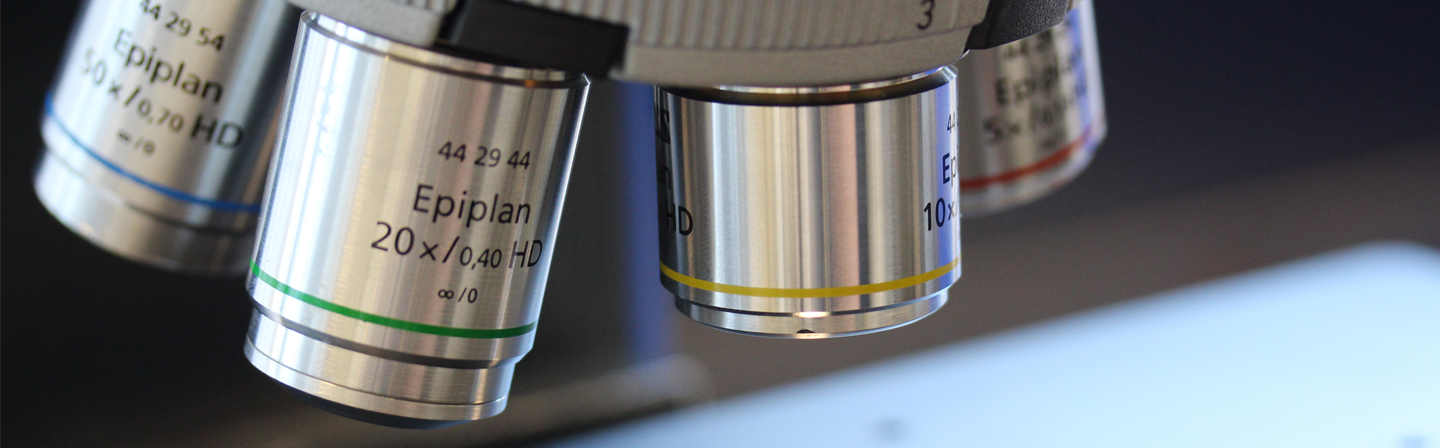
Available Characterization Methods

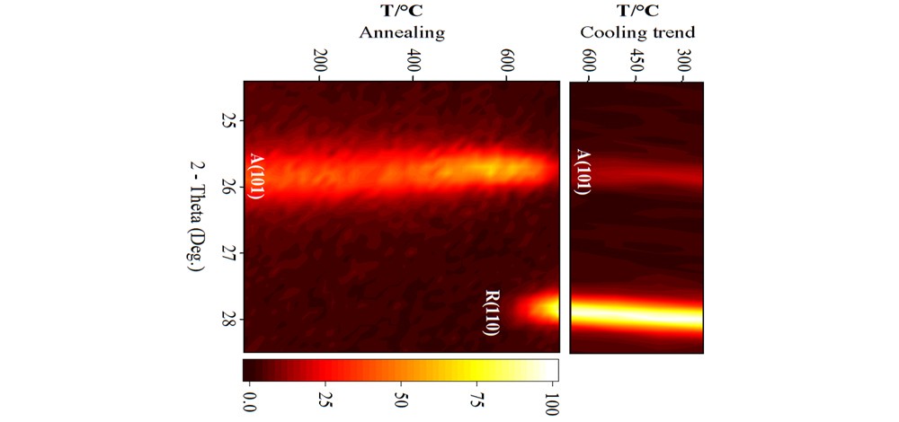
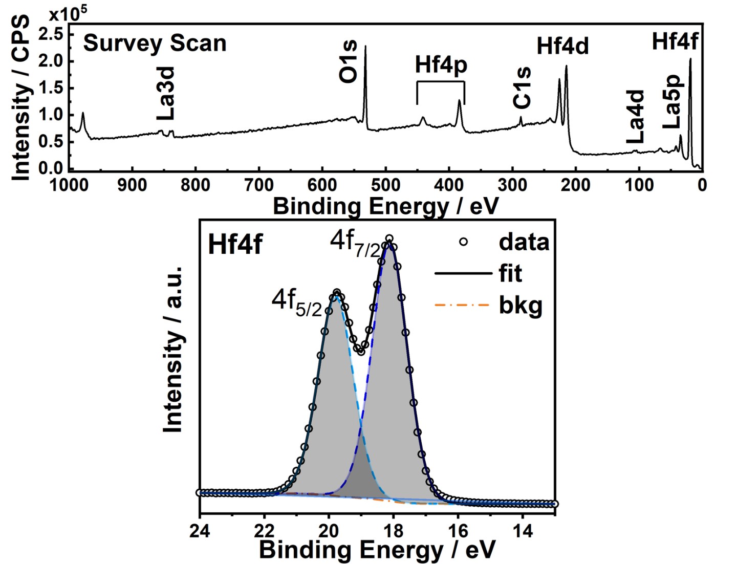
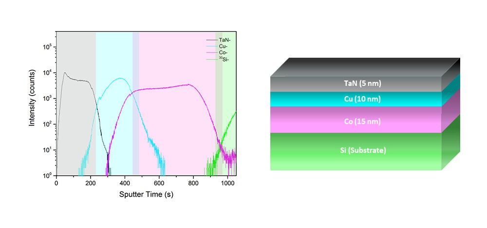
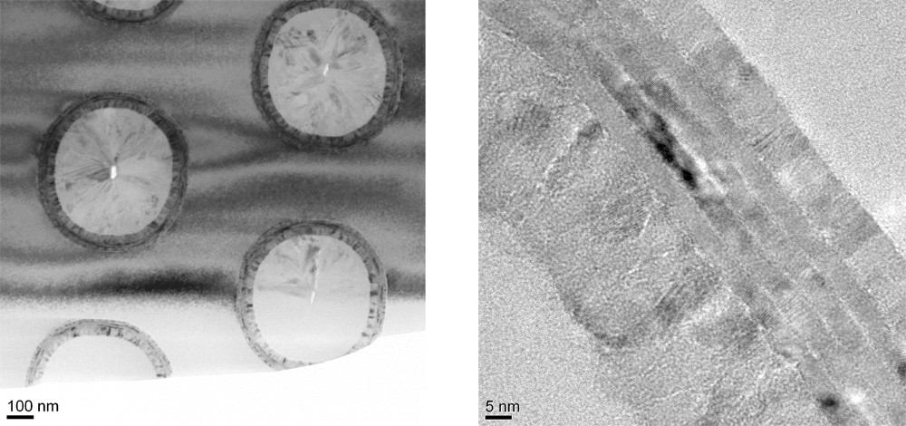
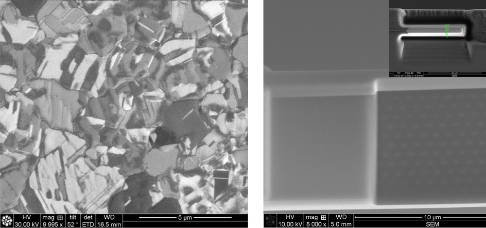
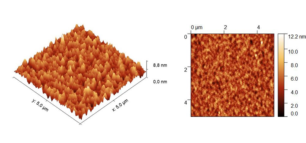
Fraunhofer IPMS offers a wide variety of analytical characterization methods in our physical failure analysis labs. We focus on wafer characterization using various X-ray methods (XPS, XRD/XRR, and TXRF), as well as Raman spectroscopy and ToF-SIMS. Furthermore, high resolution electron microscopy (SEM, TEM with EDX, EFTEM, EELS) and grain analysis (EBSD/TKD) with corresponding preparation techniques (FIB, Precision Ion Polish, Mechanical preparation) are available. Atomic and Piezoelectric force microscopy (AFM/PFM) as well as chemical etching of wafer surfaces complements the portfolio. In addition, complete electrical characterization is available here.

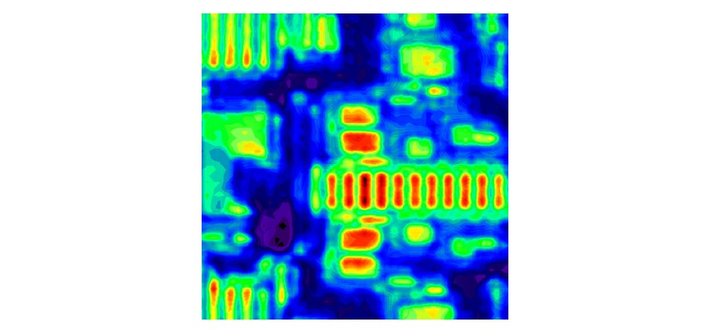
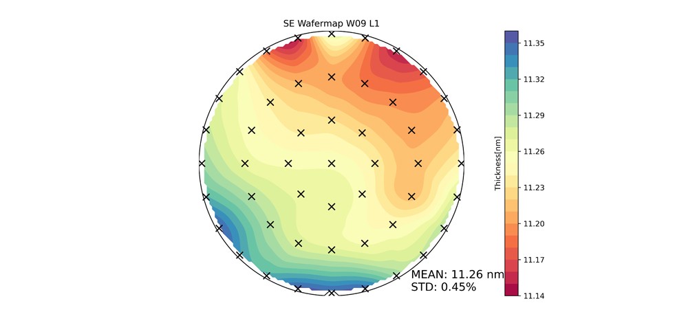
Our in-line metrology enables us to determine physical and chemical properties of structures on 300 mm wafers with, for example, X-ray diffraction, angle-resolved X-ray photoelectron spectroscopy, spectral ellipsometry and energy dispersive X-ray spectroscopy. All our tools for wafer level analysis are stationed in a class 1000 (class 6 ISO 14644-1) cleanroom environment that meets industrial standards.

X-ray Scattering

X-ray Diffraction and X-ray Reflectometry

© Fraunhofer IPMS
XRD 2D map of temperature dependent phase change.

X-ray scattering probes the arrangement of atoms in a sample by utilizing the interference of X-rays scattered at lattice planes or interfaces. It provides information about structural properties (e.g. crystallographic phases, lattice constants, degree of crystallization) and microstructural properties (e.g. grain size, preferred orientation, stress, film thickness, roughness, density). The penetration depth can be varied between a few nanometers and several micrometers. The sensitivity is about 1% phase content. The method allows for non-ambient measurements.


Capabilities

  • EPI layer characterization 
  • Growth kinetics of e.g. Hf(Si)O2 films 
  • Texture analysis of e.g. tungsten layers showing different CMP behavior 
  • Crystallization of of e.g. TiO2 thin film
  • High temperature XRD


Tool

  • Bruker D8 Discover

X-ray Photoelectron Spectroscopy

© Fraunhofer IPMS
XPS survey spectrum (top) of a HfO2 thin film showing elemental peaks and corresponding Hf4f region showing peak fit (bottom).

X-ray photoelectron spectroscopy is a quantitative technique that probes the chemistry of a material. When the X-ray source impinges a sample, electrons are excited by the photoelectric effect. The energies of the photoelectrons ejected are analyzed to obtain information on the chemical state and elemental composition of a sample. We offer a unique lab-based combination of monochromatic X-ray sources: a soft X-ray source (Aluminium Kα) and a high energy X-ray source (HAXPES using Cr Kα) for a wider range of analysis needs. The Cr Kα source offers a wider measurement range and a deeper analysis depth of about 3 times larger than with the Al Kα source. In addition, using Cr Kα, depth profiling of buried layers can be achieved without the need for ion beam sputtering, thereby avoiding ion-based degradation.

The X-ray excitation sources‘ beam sizes can be focused between 7 and 200 μm in diameter, giving way to microprobe analysis where points, lines, and mapping areas can be defined. Angle and sputter profiling depth analysis determines material composition across layer stacks or bulk material. Sample imaging using the X-ray sources is possible to create SEM-like images for the analysis of structured and inhomogeneous surfaces. In addition, in-situ XPS temperature dependent measurements can be performed in the range: -120 °C to +300 °C.


Capabilities

  • Dual monochromatic excitation: AlKα and CrKα x-ray sources
  • Unique depth profiling capabilities
  • Define various analysis areas down to tens of microns in size
  • Structured sample analysis with the help of x-ray induced secondary electron imaging (SXI)
  • In-situ temperature dependent measurements
  • Determination of chemical composition


Tools

  • PHI Quantes Scanning XPS/HAXPES Microprobe

Time-Of-Flight Secondary Ion Mass Spectrometry (ToF-SIMS)

© Fraunhofer IPMS
ToF-SIMS Graph (left) and ToF-SIMS Scheme (right).

In time-of-flight secondary ion mass spectrometry (ToF-SIMS), a primary ion beam is used to produce monatomic and polyatomic particles (secondary ions) from the sample surface. The technique is used to characterize the surface and sub-surface region of materials based on m/z ratio measurement of ejected particles under ion bombardment. The mass of the emitted ions is analyzed using a mass spectrometer. As the ion beam creates a crater in the sample, the distribution of different species within the sample volume can be recorded. We can achieve a lateral resolution of a few hundred nanometers and a depth resolution of a few monolayers. In order to quantify the absolute concentration of the elements in the sample, it is necessary to compare the analysis results to standards.


Capabilities

  • Analysis of a RRAM stack
  • Diffusion of Si in AL2O3


Tool

  • ION-TOF TOF.SIMS 300R

Electron Microscopy

© Fraunhofer IPMS
TEM bright field (left) and TEM bright field zoomed in (right).

Electron microscopy uses an electron beam to illuminate a specimen and create a magnified image. Two different types of electron microscopes are available: scanning electron microscopes (SEM, resolution down to ~1 nm) and transmission electron microscopes (TEM, resolution down to 0.1 nm). In SEM the electron beam is scanned over the sample and either the emitted secondary electrons or the back scattered electron are used for imaging the sample surface. In TEM the electron beam is passed through a thin lamella containing the region of interest. 

At our SEM complementary element and grain analysis by means of EDX & EBSD/TKD is possible. Due to the arrangement of the attached detectors both methods can be carried out simultaneously. Where the EDX analysis unfolds the elemental composition, grain analysis gives information about the crystallographic structure & possible texture. Transmission Kikuchi diffraction (TKD) adds thereby the capability of analyzing nanostructured materials & thin films on electron-transparent lamellae, whereas EBSD analysis is carried out on larger areas on the bulk material.

The emerging beam carries information about the structure of the sample that can be evaluated in different ways. On our TEM there are six different ways we can utilize the information created by the transmission electron beam:

  • Bright field imaging / Dark field imaging
  • High angle annular dark-field scanning 
  • TEM (HAADF-STEM)
  • Energy dispersive X-ray spectroscopy (EDX)
  • Electron energy loss spectroscopy (EELS) and 
  • Energy-filtered TEM (EFTEM).


Capabilities

  • Evaluation of an etching process
  • Physical failure analysis
  • HAADF-STEM 
  • EDX profiling of thin film stacks
  • EBSD/TKD
  • EFTEM


Tools

  • Thermo Fisher Apreo S
  • Hitachi S5000
  • FEI Tecnai F20

Focused Ion Beam

© Fraunhofer IPMS
Cu grain structure of electroplated Cu on a silicon wafer (left) and formation of a lamellae. The ROI is covered by protective layers of C and Pt, dug out with the beam, placed on a grid, thinned until electron transparent (right and upper right corner).

Focused Ion Beam is an essential tool in modern physical failure analysis. A finely focused ion beam allows for precise cutting into a sample. This tool is indispensable for the site-specific preparation of TEM lamellae and EBSD/TKD samples. FIB tools nowadays are usually dual-beam machines equipped with both an ion beam column and an electron beam column; hence images with electrons and ions can be taken in parallel. In addition our tool is equipped with a micromanipulator and a platinum, as well as a carbon gas injection system allowing for local deposition of platinum and carbon respectively. As a result the apparatus can furthermore be utilized for nanolithography and circuit modification.


Capabilities

  • Preparation of electron transparent lamellae for TEM or TKD
  • Ion beam imaging
  • Preparation of cross-section cuts of wafers for evaluation e.g. deposition & etching regimes as well as failure analysis


Tool

  • FEI Strata 400

Light Microscopy

Full wafer light microscopy allows images of the whole wafer. Vacuum mounting for 200 mm and 300 mm wafers ensures best handling and stable acquisition of images. Automatic data acquisition of predefined wafer areas or the full wafer is done with automatic stage movement and z-direction stacks (EDF function). Magnifications reaching from 2.5x (overview) up to 150x are possible. The extended focus function allows sharp images even of specimens with very high topologies. Dedicated areas (zoom) and position recognition is also available.


Capabilities

  • Bright field / Dark field / Differential 
  • Interference Contrast in circularly polarized light (C-DIC)
  • 200/300 mm wafers, smaller pieces
  • Motorized focus drive (5nm) and motorized x-y-scanning stage


Tools

  • Zeiss Axio Imager KMAT
  • Axio Imager.A1m

Atomic Force Microscopy

© Fraunhofer IPMS
AFM in topography mode for surface roughness analysis and corresponding 3D profile.

Our lab AFM from Oxford Instruments  is additionally equipped with PFM (piezo force microscopy) and C-AFM (conductive AFM) modes. Normally we process tapping/non-contact mode for surface roughness analysis in air. Our field of view is 30 x 30 µm2, and typical sample sizes are 1 x 1 cm2. Roughness or levels can be selected between 3 nm and 1 µm.


Capabilities

  • Topography (AFM standard)
  • C-AFM
  • PFM


Tool

  • Oxford Instruments Asylum Research Cypher

Raman Spectroscopy

© Fraunhofer IPMS
Silicon stress map in microchip pattern obtained by Raman microscopy, sample size 10 x 10 µm (red = compressive, blue = tensile stress).

Raman spectroscopy utilizes inelastic scattering of laser light to locally excite and image characteristic vibrational modes in a material. This scattering process involves the excitation or decay of characteristic vibrations of chemical bonds. As a result Raman spectroscopy can be used for the analysis of the orientation, phase and composition of a material as well as or lateral resolved stress and temperature mappings. Our tools allow for a lateral resolution down to 300 nm. Different lasers allow us to vary the surface sensitivity, varying the integration depth from only a few nanometers to a few micrometers.


Capabilities

  • Stress maps of trenches (top down & cross section)
  • Laterally resolved temperature measurements
  • Laterally resolved phase analysis


Tool

  • Renishaw Invia Reflex

Inline Metrology

© Fraunhofer IPMS
2D thickness map of a 10 nm Al2O3 film.

Physical and chemical characterization of full wafers with high throughput without affecting the functionality of the wafer dies is a key to monitor the production of semiconductor devices. At Fraunhofer IPMS we have a number of different in-line metrology tools for the measurement of film thicknesses, sheet resistance, surface composition, chemical binding states, surface and sidewall topographies and for defect inspection on 200 and 300 mm wafers.


Capabilities

  • Surface composition wafer-mapping (Thermo Fisher Theta300i ARXPS)
  • Profilometry and 3D-AFM (KLA Tencor HRP340 & Bruker Nano X3D)
  • XRD (Bede HR, video system, micro focus X-ray tube)
  • Defect inspection (KLA Tencor SP3 SurfScan & Applied Materials G3E FIB, AMAT Verity CD SEM, NextIn Solutions AEGIS Wafer Inspection System)
  • Film thickness wafer-mapping (KLA Tencor Spectra FX100)
  • Sheet resistivity (EURIS WS3000 & KLA Tencor RS100)

Further Information:

Data sheet

300 mm Process Catalogue