 Fraunhofer Institute for Photonic Microsystems
Fraunhofer IPMS - Center Nanoelectronic Technologies cooperates with South Korean technology company NextIn
The Fraunhofer Institute for Photonic Microsystems (Fraunhofer IPMS) has entered into a collaborative relationship with South Korean semiconductor equipment manufacturer NextIn. As part of the one-year cooperative effort, a new defect inspection system will be evaluated in the clean room of Center Nanoelectronic Technologies (CNT); the tool allows for the visual detection, automatic classification and characterization of different defect types on structured wafers (200 mm and 300 mm).
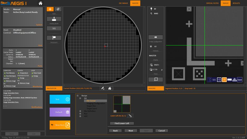
The NextIn Aegis I Wafer Inspection System makes it possible to combine bright field and dark field imaging in one tool, which significantly increases the number of different applications in semiconductor research and development. Once the evaluation has been completed, NextIn will therefore offer a flexible metrology tool for the 2x nm technology node.
»As a research institution, this project creates synergy effects because this type of equipment is very important for the research and development of FEoL, MoL and BEoL processes. Additionally, this collaboration serves to expand our business relationships into Asia.« says Dr. Benjamin Uhlig, head of the Interconnects group at business unit CNT.
Thus, the Center Nanoelectronic Technologies is continuing the successful collaboration between the semiconductor industry and applied science in the segment of 300 mm wafer technology, which allows manufacturers to implement new developments at the industrial level.
About Fraunhofer IPMS - Center Nanoelectronic Technologies (CNT)
With 23,000 employees, the Fraunhofer-Gesellschaft is Europe's largest research organization for applied research. Fraunhofer IPMS is one of 67 facilities and serves as an example of the close collaboration between applied science and semiconductor production sites within the »Silicon Saxony« economic region. The competencies of the business unit CNT are focused on nanoelectronic processes and products. A 800 m² clean room and more than 40 process and analytical tools for 200 and 300 mm wafers are available. Due to the industry standard developments and new processes can be quickly integrated into production lines.
About NextIn
NEXTIN Inc. is a South Korean manufacturer of defect inspection equipment for semiconductor and FPD industries. Its high-caliber tools helps customers manage their yield on all process steps at the most advanced design nodes.