 Fraunhofer Institute for Photonic Microsystems
At Semicon Europe the Fraunhofer Institute for Photonic Microsystems competes for small and medium sized companies

The Fraunhofer IPMS carries out customer specific developments in fields of microelectronic and micro systems technology in Dresden, serving as a business partner that supports the transition of innovative ideas into new products. The Fraunhofer IPMS develops and fabricates modern CMOS technology products in its own clean room facilities, up to small pilot series production. With modern equipment and about 240 scientists, the range of projects and expertise covers sensor and actuator systems, microscanner, spatial light modulators, lifetronics and organic materials and systems.
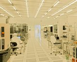
The Fraunhofer Institute for Photonic Microsystems (Fraunhofer IPMS) features almost everything needed for the development, fabrication and integration of technologies for micro-electro-mechanical systems (MEMS) and micro-opto-electro-mechanical systems (MOEMS): outstanding technology know-how, expertise in industrial manufacturing projects and the infrastructure needed including state-of-the-art equipment and 1500 m² class 10 clean room facilities. Using this potential at the Semicon Europe show in Dresden from October 06 to October 08 the institute wants to attract potential customers with a special focus on small and medium companies.
Nowadays MEMS devices with diverse features can be found in a great deal of products such as printing machines, automotive vehicles, mobile phones or computers. They are used as sensors for process management and quality equipment as well as for telecommunication or medical technology. The approach of the scientists from Fraunhofer to compete for small and medium sized companies at the Semicon Europe show is because of recent investments in modern infrastructure on the one hand and the increasing demand for specific process modules for MEMS development and fabrication on the other. »Before the new MEMS clean room was completed in summer 2007 we were working to full capacity on volume production projects as well as the development of micro scanning mirrors and spatial light modulators«, says director of the Fraunhofer IPMS Prof. Dr. Hubert Lakner. »However growing clean room space and the investment in modern equipment allow us to accept and quickly deal with orders like a MEMS foundry. We aim to particularly support small and medium sized companies without the needed equipment or facilities to bring their innovative products to the market.«
In order to learn more about these new opportunities for MEMS development and fabrication the Fraunhofer IPMS invites all Semicon visitors to attend a presentation in the Semicon TechArena on October 7 at 02:45 p.m. and to join a guided company tour through the clean room and showroom of the institute for product demonstrations on the first two days of the show, on October 6 and 7. Meeting point for the two hour lasting tour is the Fraunhofer IPMS' exhibition booth 4.116 in hall 4 at 2:00 p.m. The number of attendies is limited to 20 people. A shuttle transfer to the institute and the way back is organized.